SLUSD36 September 2017
PRODUCTION DATA.
- 1 Features
- 2 Applications
- 3 Description
- 4 Revision History
- 5 Description (continued)
- 6 Pin Configuration and Functions
- 7 Specifications
-
8 Detailed Description
- 8.1 Overview
- 8.2 Functional Block Diagram
- 8.3
Feature Description
- 8.3.1 Power-On-Reset (POR)
- 8.3.2 Device Power Up from Battery without Input Source
- 8.3.3 Power Up from Input Source
- 8.3.4 Host Mode and Standalone Power Management
- 8.3.5 Power Path Management
- 8.3.6 Battery Charging Management
- 8.3.7 Shipping Mode
- 8.3.8 Status Outputs (PG, STAT)
- 8.3.9 Protections
- 8.3.10 Serial interface
- 8.4 Register Maps
- 9 Application and Implementation
- 10Power Supply Recommendations
- 11Layout
- 12Device and Documentation Support
- 13Mechanical, Packaging, and Orderable Information
Package Options
Mechanical Data (Package|Pins)
- YFF|30
Thermal pad, mechanical data (Package|Pins)
Orderable Information
1 Features
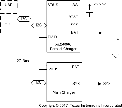
- Operation as Parallel Charger to Provide Fast Charging in Dual Charger Operation
- High-Efficiency, 1.5-MHz, Synchronous Switch-Mode Buck Charger
- 92% Charge Efficiency at 2 A from 5-V Input
- Optimized for USB Voltage Input (5 V)
- Low Power Pulse Frequency Modulation (PFM) Mode for Light Load Operations
- Single Input to Support USB Input and High Voltage Adapters
- Support 3.9-V to 13.5-V Input Voltage Range With 22-V Absolute Maximum Input Voltage Rating
- Programmable Input Current Limit (100 mA to 3.2 A With 100-mA Resolution) to Support USB 2.0, USB 3.0 Standards and High Voltage Adaptors (IINDPM)
- Maximum Power Tracking by Input Voltage Limit Up to 5.4 V (VINDPM)
- VINDPM Threshold Automatically Tracks Battery Voltage
- High Charge Efficiency With 19.5-mΩ Charging Current Sensing MOSFET
- Narrow VDC (NVDC) Power Path Management
- Instant-On Works with No Battery or Deeply Discharged Battery
- Ideal Diode Operation in Battery Supplement Mode
- Flexible Autonomous and I2C Mode for Optimal System Performance
- High Integration Includes All MOSFETs, Current Sensing and Loop Compensation
- 17-µA Low Battery Leakage Current
- High Accuracy
- ±0.5% Charge Voltage Regulation
- ±5% at 1.5-A Charge Current Regulation
- ±6% at 1.38-A Charge Current Regulation
- ±10% at 0.9-A Input Current Regulation
- Remote Battery Sensing for Fast Charge
2 Applications
- Smart Phones
- Tablet
3 Description
The bq25600C devices are highly-integrated 3.0-A switch-mode battery charge management and system power path management device for single cell Li-Ion and Li-polymer battery. The low impedance power path optimizes switch-mode operation efficiency and reduces battery charging time. The I2C serial interface with charging and system settings makes the device a truly flexible solution.
Device Information(1)
| PART NUMBER | PACKAGE | BODY SIZE (NOM) |
|---|---|---|
| bq25600C | DSBGA (30) | 2.2 mm × 2.59 mm |
- For all available packages, see the orderable addendum at the end of the data sheet.
Simplified Schematic
