SLUSCQ6 October 2016
PRODUCTION DATA.
- 1 Features
- 2 Applications
- 3 Description
- 4 Revision History
- 5 Pin Configuration and Functions
- 6 Specifications
- 7 Typical Characteristics
-
8 Detailed Description
- 8.1 Overview
- 8.2 Functional Block Diagram
- 8.3
Feature Description
- 8.3.1 Device Power Up
- 8.3.2 Battery Switch (Q1 + Q2)
- 8.3.3 Integrated 10-bit ADC for Monitoring
- 8.3.4 Linear Regulation Mode (LDO)
- 8.3.5
Protection Features
- 8.3.5.1 Reverse Current Protection (RCP)
- 8.3.5.2 Internal Thermal Shutdown
- 8.3.5.3 Input Overvoltage Protection
- 8.3.5.4 IBUS and VBUS Protection
- 8.3.5.5 IBAT and VBAT Protection
- 8.3.5.6 VOUT Protection
- 8.3.5.7 VDROP Protection
- 8.3.5.8 VBUS Temperature (TS_BUS_FLT) and Battery Temperature (TS_BAT_FLT)
- 8.3.6 I2C Serial Interface
- 8.4 Device Functional Modes
- 8.5
I2C Register Maps
- 8.5.1 I2C Register Summary Table
- 8.5.2 REG00 (DEVICE_INFO)
- 8.5.3 REG01 (EVENT_1_MASK)
- 8.5.4 REG02 (EVENT_2_MASK)
- 8.5.5 REG03 (EVENT_1)
- 8.5.6 REG04 (EVENT_2)
- 8.5.7 REG05 (EVENT_1_EN)
- 8.5.8 REG06 (CONTROL)
- 8.5.9 REG07 (ADC_CONTROL)
- 8.5.10 REG08 (ADC_EN)
- 8.5.11 REG09 (PROTECTION)
- 8.5.12 REG0A (VBUS_OVP)
- 8.5.13 REG0B (VOUT_REG)
- 8.5.14 REG0C (VDROP_OVP)
- 8.5.15 REG0D (VDROP_ALM)
- 8.5.16 REG0E (VBAT_REG)
- 8.5.17 REG0F (IBAT_REG)
- 8.5.18 REG10 (IBUS_REG)
- 8.5.19 REG11 (TS_BUS_FLT)
- 8.5.20 REG12 (TS_BAT_FLT)
- 8.5.21 REG 13 and REG 14 (VBUS_ADC)
- 8.5.22 REG15 and REG16 (IBUS_ADC)
- 8.5.23 REG17 and REG18 (VOUT_ADC)
- 8.5.24 REG19 and REG1A (VDROP_ADC)
- 8.5.25 REG1B and REG1C (VBAT_ADC)
- 8.5.26 REG1D and REG1E (IBAT_ADC)
- 8.5.27 REG1F and REG20 (TS_BUS_ADC)
- 8.5.28 REG21 and REG22 (TS_BAT_ADC)
- 8.5.29 REG 23 (TDIE_ADC)
- 8.5.30 REG 24 (EVENT_2_EN)
- 8.5.31 REG 25 (EVENT_3_MASK)
- 8.5.32 REG 26 (EVENT_3)
- 8.5.33 REG27 and REG28 (VUSB_ADC)
- 8.5.34 REG 29 (CONTROL_2)
- 8.5.35 REG 40 (DIE_TEMP_FLT)
- 9 Application and Implementation
- 10Power Supply Recommendations
- 11Layout
- 12Device and Documentation Support
- 13Mechanical, Packaging, and Orderable Information
Package Options
Refer to the PDF data sheet for device specific package drawings
Mechanical Data (Package|Pins)
- YFF|42
Thermal pad, mechanical data (Package|Pins)
Orderable Information
1 Features
- Adapter Input Voltage Range: 3 V to 14 V
- Allow up to 14-V Adaptor Voltage
- Highly Integrated 7-A Battery Switch
- Integrated MOSFETs and Current Sensing
- Low RDS(on) (13-mΩ) MOSFETs for High Current Operation
- Integrated High Accuracy ADC for System Monitor
- VBUS, VBAT, VOUT, VDROP Voltage
- Input and Battery Current
- Battery and VBUS Connector Temperature
- Linear Regulation (LDO) Mode Operation
- Four Linear Regulation Loops: IBUS, IBAT, VBAT and VOUT
- Programmable Linear Regulation Thresholds
- Programmable Safety Protections
- VBUS, VOUT, and VBAT Over Voltage Protections (OVP)
- IBUS and IBAT Over Current Protection (OCP)
- IBUS Reverse Current Protection (RCP)
- VDROP (VBUS-VOUT) OVP
- VBUS Connector and Battery Thermal Protection
- Thermal Shutdown
- Integrated Input OVP FET Control with Fast OVP Response (2 µs)
- Interrupt Status Output For Host Processor Alert
- Up To 1-MHz I2C Read and Write Speed
- Low Battery Leakage Current in Battery Only Mode
- WCSP Package for Small Footprint
2 Applications
- Smart Phone
- Tablet PC
3 Description
The device is a 7-A battery switch charger with an integrated 10-bit ADC. The high-current battery switch charger is a 13-mΩ MOSFET with reverse current blocking designed for high efficiency and minimal voltage drop. The high-charge current capability of the device makes it ideal for smartphones, tablets, and other portable devices with large battery capacity.
The integrated 10-bit ADC can measure input voltage and current, battery voltage and current, as well as battery temperature and input connector temperature. This allows the user application to continuously monitor the power input and battery charging parameters to ensure the safety of the battery charging. The flexible OVP and OCP thresholds for VBUS, VOUT, and battery can be modified via I2C registers as the battery goes through constant current (CC) and constant voltage (CV) mode.
The I2C serial interface of the device can operate at speeds up to 1 MHz and allows access to the ADC’s measurements of the different charging parameters and also allows for flexible software control of the device. The INT pin provides instantaneous feedback to the host in case of a fault condition. I2C status registers allow the host to read the current status of all faults and events.
The device comes in a DSBGA package.
Device Information(1)
| PART NUMBER | PACKAGE | BODY SIZE (NOM) |
|---|---|---|
| bq25872 | YFF (42) | 2.5 mm x 3.1 mm |
- For all available packages, see the orderable addendum at the end of the data sheet.
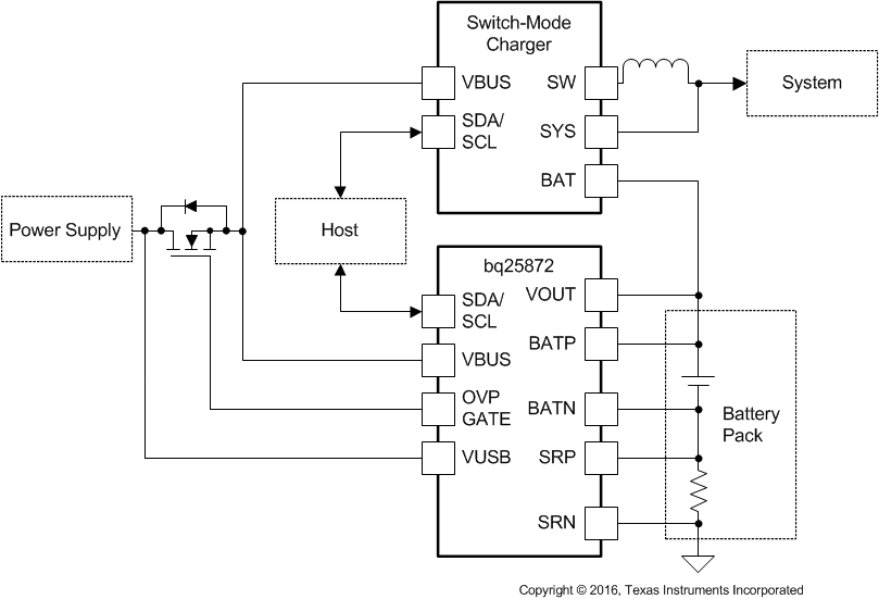
Simplified Schematic

4 Revision History
| DATE | REVISION | NOTES |
|---|---|---|
| October 2016 | * | Initial release. |