SLUSCA6B March 2016 – March 2017
PRODUCTION DATA.
- 1 Features
- 2 Applications
- 3 Description
- 4 Revision History
- 5 Description (Continued)
- 6 Device Comparison Table
- 7 Pin Configuration and Functions
- 8 Specifications
-
9 Detailed Description
- 9.1 Functional Block Diagram
- 9.2
Feature Description
- 9.2.1 Device Power-On-Reset (POR)
- 9.2.2 Device Power Up from Battery without Input Source
- 9.2.3 Device Power Up from Input Source
- 9.2.4 Input Current Optimizer (ICO)
- 9.2.5 Boost Mode Operation from Battery
- 9.2.6 Power Path Management
- 9.2.7 Battery Charging Management
- 9.2.8 Battery Monitor
- 9.2.9 Status Outputs (PG, STAT, and INT)
- 9.2.10 BATFET (Q4) Control
- 9.2.11 Current Pulse Control Protocol
- 9.2.12 Input Current Limit on ILIM
- 9.2.13 Thermal Regulation and Thermal Shutdown
- 9.2.14 Voltage and Current Monitoring in Buck and Boost Mode
- 9.2.15 Battery Protection
- 9.2.16 Serial Interface
- 9.3 Device Functional Modes
- 9.4 Register Map
- 10Application and Implementation
- 11Power Supply Recommendations
- 12Layout
- 13Device and Documentation Support
- 14Mechanical, Packaging, and Orderable Information
Package Options
Refer to the PDF data sheet for device specific package drawings
Mechanical Data (Package|Pins)
- YFF|42
Thermal pad, mechanical data (Package|Pins)
Orderable Information
1 Features
- High Efficiency 4-A, 1.5-MHz Switch Mode Buck Charge
- 92% Charge Efficiency at 3 A and 91% Charge Efficiency at 4 A Charge Current
- Optimize for High Voltage Input (9 V / 12 V)
- Low Power PFM mode for Light Load Operations
- USB On-the-Go (OTG) with Adjustable Output from 4.5 V to 5.5 V
- Single Input to Support USB Input and Adjustable High Voltage Adapters
- Support 3.9-V to 14-V Input Voltage Range
- Input Current Limit (100 mA to 3.25 A with 50-mA resolution) to Support USB2.0, USB3.0 standard and High Voltage Adapters
- Maximum Power Tracking by Input Voltage Limit up-to 14V for Wide Range of Adapters
- Auto Detect USB SDP, CDP, DCP, and Non-Standard Adapters (bq25898)
- Programmable D+/D- Drivers for Non-Standard Adapter Handshake
- Remote Battery Sensing
- Input Current Optimizer (ICO) to Maximize Input Power without Overloading Adapters
- Resistance Compensation (IRCOMP) from Charger Output to Cell Terminal
- Highest Battery Discharge Efficiency with 5-mΩ Battery Discharge MOSFET up to 9 A
- Integrated ADC for System Monitor
(Voltage, Temperature, Charge Current) - Narrow VDC (NVDC) Power Path Management
- Instant-on Works with No Battery or Deeply Discharged Battery
- Ideal Diode Operation in Battery Supplement Mode
- BATFET Control to Support Ship Mode, Wake Up, and Full System Reset
- Flexible Autonomous and I2C Mode for Optimal System Performance
- High Integration includes all MOSFETs, Current Sensing and Loop Compensation
- 12-µA Low Battery Leakage Current to Support Ship Mode
- High Accuracy
- ±0.5% Charge Voltage Regulation
- ±5% Charge Current Regulation
- ±7.5% Input Current Regulation
- Safety
- Battery Temperature Sensing for Charge and Boost Mode
- Thermal Regulation and Thermal Shutdown
- Available in 2.8-mm x 2.5-mm 42-Ball DSBGA Package
2 Applications
- Smart Phone
- Tablet PC
- Portable Internet Devices
3 Description
The bq25898, bq25898D are highly-integrated 4-A switch-mode battery charge management and system power path management devices for single cell Li-Ion and Li-polymer battery. The devices support high input voltage fast charging.
Device Information(1)
| PART NUMBER | PACKAGE | BODY SIZE (NOM) |
|---|---|---|
| bq25898 | DSBGA (42) | 2.80 mm x 2.50 mm |
| bq25898D | DSBGA (42) | 2.80 mm x 2.50 mm |
- For all available packages, see the orderable addendum at the end of the data sheet.
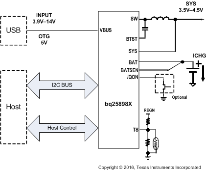
Simplified Schematic

4 Revision History
Changes from A Revision (December 2016) to B Revision
- Full data sheet to product folder Go
Changes from * Revision (March 2016) to A Revision
- Changed 93% to 94% in FeaturesGo
- Changed anode to cathode in BTSTGo
- Changed cathode to anode in REGNGo
- Changed falling to rising in tACOV_RISING test conditions in Electrical CharacteristicsGo
- Deleted USB SDP (USB100) and the OTG Pin column from Table 3 and Table 4Go
- Changed VREF to VREGN in Equation 2 Go
- Changed VREF to VREGN in Figure 18 Go
- Changed 260 Ω to 232 Ω in Input Current Limit on ILIM Go
- Added note to Figure 49 Go