SLUSCA6B March 2016 – March 2017
PRODUCTION DATA.
- 1 Features
- 2 Applications
- 3 Description
- 4 Revision History
- 5 Description (Continued)
- 6 Device Comparison Table
- 7 Pin Configuration and Functions
- 8 Specifications
-
9 Detailed Description
- 9.1 Functional Block Diagram
- 9.2
Feature Description
- 9.2.1 Device Power-On-Reset (POR)
- 9.2.2 Device Power Up from Battery without Input Source
- 9.2.3 Device Power Up from Input Source
- 9.2.4 Input Current Optimizer (ICO)
- 9.2.5 Boost Mode Operation from Battery
- 9.2.6 Power Path Management
- 9.2.7 Battery Charging Management
- 9.2.8 Battery Monitor
- 9.2.9 Status Outputs (PG, STAT, and INT)
- 9.2.10 BATFET (Q4) Control
- 9.2.11 Current Pulse Control Protocol
- 9.2.12 Input Current Limit on ILIM
- 9.2.13 Thermal Regulation and Thermal Shutdown
- 9.2.14 Voltage and Current Monitoring in Buck and Boost Mode
- 9.2.15 Battery Protection
- 9.2.16 Serial Interface
- 9.3 Device Functional Modes
- 9.4 Register Map
- 10Application and Implementation
- 11Power Supply Recommendations
- 12Layout
- 13Device and Documentation Support
- 14Mechanical, Packaging, and Orderable Information
Package Options
Refer to the PDF data sheet for device specific package drawings
Mechanical Data (Package|Pins)
- YFF|42
Thermal pad, mechanical data (Package|Pins)
Orderable Information
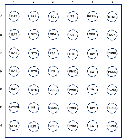
7 Pin Configuration and Functions
bq25898
YFF Package 42-Pin DSBGA
Top View

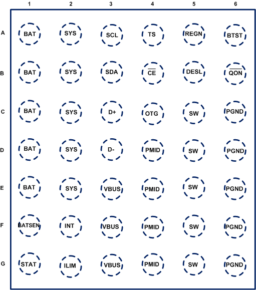
bq25898D
YFF Package 42-Pin DSBGA
Top View

Pin Functions
| PIN | TYPE(1) | DESCRIPTION | ||
|---|---|---|---|---|
| NAME | bq25898 | bq25898D | ||
| VBUS | E3-G3 | E3-G3 | P | Charger Input Voltage. The internal n-channel reverse block MOSFET (RBFET) is connected between VBUS and PMID with VBUS on source. Place a 1-µF ceramic capacitor from VBUS to PGND and place it as close as possible to IC. |
| D+ | – | C3 | AIO | Positive line of the USB data line pair. D+/D- based USB host/charging port detection. The detection includes data contact detection (DCD), primary and secondary detection in BC1.2, and Adjustable high voltage adapter. |
| PSEL | C3 | – | DI | Power source selection input. High indicates a USB host source and Low indicates an adapter source. |
| D– | – | D3 | AIO | Negative line of the USB data line pair. D+/D- based USB host/charging port detection. The detection includes data contact detection (DCD), primary and secondary detection in BC1.2, and Adjustable high voltage adapter. |
| PG | D3 | – | DO | Open drain active low power good indicator. Connect to the pull up rail via 10-kΩ resistor. LOW indicates a good input source if the input voltage is within VVBUS_OP, above SLEEP mode threshold (VSLEEPZ), and current limit is above IBATSRC(30 mA). |
| STAT | G1 | G1 | DO | Open drain charge status output to indicate various charger operation. Connect to the pull up rail via 10-kΩ resistor. LOW indicates charge in progress. HIGH indicates charge complete or charge disabled. When any fault condition occurs, STAT pin blinks in 1 Hz. The STAT pin function can be disabled when STAT_DIS bit is set. |
| SCL | A3 | A3 | DI | I2C Interface clock. Connect SCL to the logic rail through a 10-kΩ resistor. |
| SDA | B3 | B3 | DIO | I2C Interface data. Connect SDA to the logic rail through a 10-kΩ resistor. |
| INT | F2 | F2 | DO | Open-drain Interrupt Output. Connect the INT to a logic rail via 10-kΩ resistor. The INT pin sends active low, 256-μs pulse to host to report charger device status and fault. |
| OTG | C4 | C4 | DI | Active high enable pin during boost mode. Deleted text form the OTG pin Description "OTG = High, IINLIM is set to USB500 mode". The boost mode is activated when OTG_CONFIG =1 and OTG pin is highChanged the Description of the OTG pin in the Pin Functions table. |
| CE | B4 | B4 | DI | Active low Charge Enable pin. Battery charging is enabled when CHG_CONFIG = 1 and CE pin = Low. CE pin must be pulled High or Low. |
| ILIM | G2 | G2 | AI | Input current limit Input. ILIM pin sets the maximum input current and can be used to monitor input current ILIM pin sets the maximum input current limit by regulating the ILIM voltage at 0.8 V. A resistor is connected from ILIM pin to ground to set the maximum limit as IINMAX = KILIM/RILIM. The actual input current limit is the lower limit set by ILIM pin (when EN_ILIM bit is high) or IIINLIM register bits. Input current limit of less than 500 mA is not support on ILIM pin. ILIM pin can also be used to monitor input current when the voltage is below 0.8V. The input current is proportional to the voltage on ILIM pin and can be calculated by IIN = (KILIM x VILIM) / (RILIM x 0.8) The ILIM pin function can be disabled when EN_ILIM bit is 0. |
| TS | A4 | A4 | AI | Temperature qualification voltage input. Connect a negative temperature coefficient thermistor. Program temperature window with a resistor divider from REGN to TS to GND. Charge suspends when either TS pin is out of range. Recommend 103AT-2 thermistor. |
| QON | B6 | B6 | DI | BATFET enable/reset control input. When BATFET is in ship mode, a logic low of tSHIPMODE (typical 1sec) duration turns on BATFET to exit shipping mode. . When VBUS is not plugged-in, a logic low of tQON_RST (typical 19.5sec) duration resets SYS (system power) by turning BATFET off for tBATFET_RST (typical 0.325sec) and then re-enable BATFET to provide full system power reset. The pin contains an internal pull-up to maintain default high logic |
| BAT | A1-E1 | A1-E1 | P | Battery connection point to the positive terminal of the battery pack. The internal BATFET is connected between BAT and SYS. Connect a 10uF closely to the BAT pin. |
| SYS | A2-E2 | A2-E2 | P | System connection point. The internal BATFET is connected between BAT and SYS. When the battery falls below the minimum system voltage, switch-mode converter keeps SYS above the minimum system voltage. Connect a 20uF closely to the SYS pin. |
| PGND | C6-G6 | C6-G6 | P | Power ground connection for high-current power converter node. |
| SW | C5-G5 | C5-G5 | P | Switching node connecting to output inductor. Internally SW is connected to the source of the n-channel HSFET and the drain of the n-channel LSFET. Connect the 0.047μF bootstrap capacitor from SW to BTST. |
| BTST | A6 | A6 | P | PWM high side driver positive supply. Internally, the BTST is connected to the cathode of the boost-strap diode. Connect the 0.047μF bootstrap capacitor from SW to BTST. |
| REGN | A5 | A5 | P | PWM low side driver positive supply output. Internally, REGN is connected to the anode of the boost-strap diode. Connect a 4.7 µF (10 V rating) ceramic capacitor from REGN to analog GND. The capacitor should be placed close to the IC. REGN also serves as bias rail of TS pin. |
| PMID | D4-G44 | D4-G4 | DO | Connected to the drain of the reverse blocking MOSFET (RBFET) and the drain of HSFET. Given the total input capacitance, put 1µF on VBUS to PGND, and the rest capacitance on PMID to PGND. |
| DSEL | – | B5 | DO | Active high D+/D- multiplexer selection control. Connect a 47-nF (6V rating) ceramic capacitor from DSEL to analog GND. The pin is normally low. During input source type detection, the pin drives high to indicate the bq25890 D+/D- detection is in progress and needs to take control of D+, D- signals. When detection is completed, the pin keeps high when DCP, MaxCharge or HVDCP is detected. The pin returns to low when other input source type is detected |
| VOK | B5 | – | DO | LDO output to driver USB PHY/MUX. Connect a 47nF ceramic capacitor from VOK to analog GND. |
| BATSEN | F1 | F1 | AI | Remote battery sense input. The typical pin resistance is 800 kΩ. Connect as close to battery as possible. |
(1) DI (Digital Input), DO (Digital Output), DIO (Digital Input/Output), AI (Analog Input), AO (Analog Output), AIO (Analog Input/Output)