SLUSBH1C November 2013 – December 2014
PRODUCTION DATA.
- 1 Features
- 2 Applications
- 3 Description
- 4 Simplified Schematic
- 5 Revision History
- 6 Device Comparison Table
- 7 Pin Configuration and Functions
-
8 Specifications
- 8.1 Absolute Maximum Ratings
- 8.2 ESD Ratings
- 8.3 Recommended Operating Conditions
- 8.4 Thermal Information
- 8.5 Supply Current
- 8.6 Digital Input and Output DC Characteristics
- 8.7 LDO Regulator, Wake-up, and Auto-Shutdown DC Characteristics
- 8.8 LDO Regulator, Wake-up, and Auto-shutdown AC Characteristics
- 8.9 ADC (Temperature and Cell Measurement) Characteristics
- 8.10 Integrating ADC (Coulomb Counter) Characteristics
- 8.11 I2C-Compatible Interface Communication Timing Characteristics
- 8.12 SHUTDOWN and WAKE-UP Timing
- 8.13 Typical Characteristics
- 9 Detailed Description
- 10Application and Implementation
- 11Power Supply Recommendation
- 12Layout
- 13Device and Documentation Support
- 14Mechanical, Packaging, and Orderable Information
Package Options
Mechanical Data (Package|Pins)
- DRZ|12
Thermal pad, mechanical data (Package|Pins)
Orderable Information
10 Application and Implementation
NOTE
Information in the following application section is not part of the TI component specification, and TI does not warrant its accuracy or completeness. TI’s customers are responsible for determining suitability of components for their purposes. Customers should validate and test their design implementation to confirm system functionality.
10.1 Application Information
The bq27441-G1 fuel gauge is a microcontroller peripheral that provides system-side fuel gauging for single-cell Li-Ion batteries. The device requires minimal configuration and uses One Time Programmable (OTP) Non-Volatile Memory (NVM). Battery fuel gauging with the fuel gauge requires connections only to PACK+ and PACK– for a removable battery pack or embedded battery circuit. To allow for optimal performance in the end application, special considerations must be taken to ensure minimization of measurement error through proper printed circuit board (PCB) board layout. Such requirements are detailed in Design Requirements.
10.2 Typical Applications
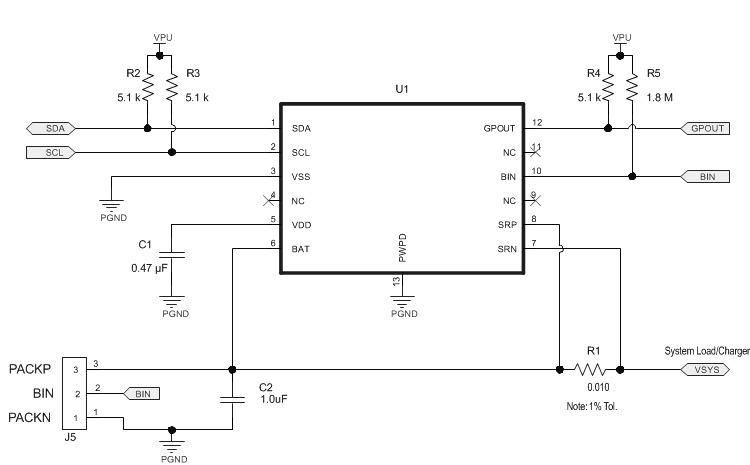 Figure 6. Typical Application
10.2.1 Design Requirements
As shipped from the Texas Instruments factory, many bq27441-G1 parameters in OTP NVM are left in the unprogrammed state (zero) while some parameters directly associated with the CHEMID are preprogrammed. This partially programmed configuration facilitates customization for each end application. Upon device reset, the contents of OTP are copied to associated volatile RAM-based Data Memory blocks. For proper operation, all parameters in RAM-based Data Memory require initialization — either by updating Data Memory parameters in a lab/evaluation situation or by programming the OTP for customer production. Chapter 6 in the bq27441-G1 Technical Reference Manual (SLUUAC9) shows the default value and a typically expected value appropriate for most of applications.
10.2.2 Detailed Design Procedure
10.2.2.1 BAT Voltage Sense Input
A ceramic capacitor at the input to the BAT pin is used to bypass AC voltage ripple to ground, greatly reducing its influence on battery voltage measurements. It proves most effective in applications with load profiles that exhibit high-frequency current pulses (that is, cell phones) but is recommended for use in all applications to reduce noise on this sensitive high-impedance measurement node.
10.2.2.2 Integrated LDO Capacitor
The fuel gauge has an integrated LDO with an output on the VDD pin of approximately 1.8 V. A capacitor of value at least 0.47 μF should be connected between the VDD pin and VSS. The capacitor should be placed close to the gauge IC and have short traces to both the VDD pin and VSS.
10.2.2.3 Sense Resistor Selection
Any variation encountered in the resistance present between the SRP and SRN pins of the fuel gauge will affect the resulting differential voltage, and derived current, it senses. As such, it is recommended to select a sense resistor with minimal tolerance and temperature coefficient of resistance (TCR) characteristics. The standard recommendation based on best compromise between performance and price is a 1% tolerance, 50 ppm drift sense resistor with a 1-W power rating.
10.2.3 Application Curves
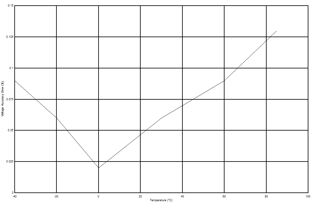 Figure 7. Voltage Accuracy
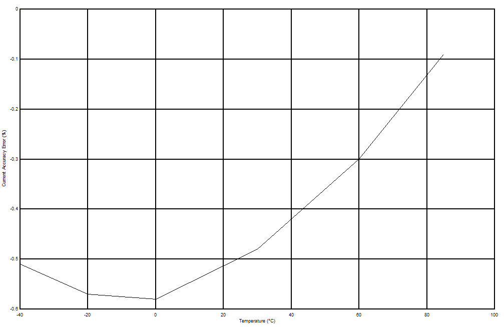 Figure 9. Current Accuracy
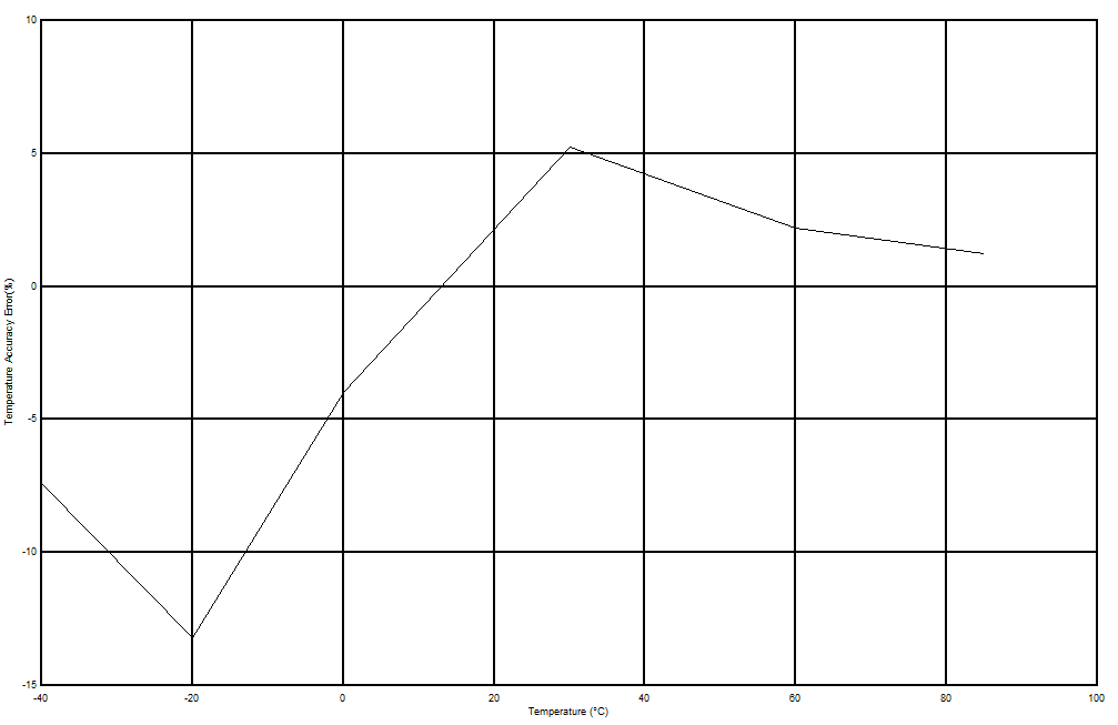 Figure 8. Temperature Accuracy