SLUSBH1C November 2013 – December 2014
PRODUCTION DATA.
- 1 Features
- 2 Applications
- 3 Description
- 4 Simplified Schematic
- 5 Revision History
- 6 Device Comparison Table
- 7 Pin Configuration and Functions
-
8 Specifications
- 8.1 Absolute Maximum Ratings
- 8.2 ESD Ratings
- 8.3 Recommended Operating Conditions
- 8.4 Thermal Information
- 8.5 Supply Current
- 8.6 Digital Input and Output DC Characteristics
- 8.7 LDO Regulator, Wake-up, and Auto-Shutdown DC Characteristics
- 8.8 LDO Regulator, Wake-up, and Auto-shutdown AC Characteristics
- 8.9 ADC (Temperature and Cell Measurement) Characteristics
- 8.10 Integrating ADC (Coulomb Counter) Characteristics
- 8.11 I2C-Compatible Interface Communication Timing Characteristics
- 8.12 SHUTDOWN and WAKE-UP Timing
- 8.13 Typical Characteristics
- 9 Detailed Description
- 10Application and Implementation
- 11Power Supply Recommendation
- 12Layout
- 13Device and Documentation Support
- 14Mechanical, Packaging, and Orderable Information
Package Options
Mechanical Data (Package|Pins)
- DRZ|12
Thermal pad, mechanical data (Package|Pins)
Orderable Information
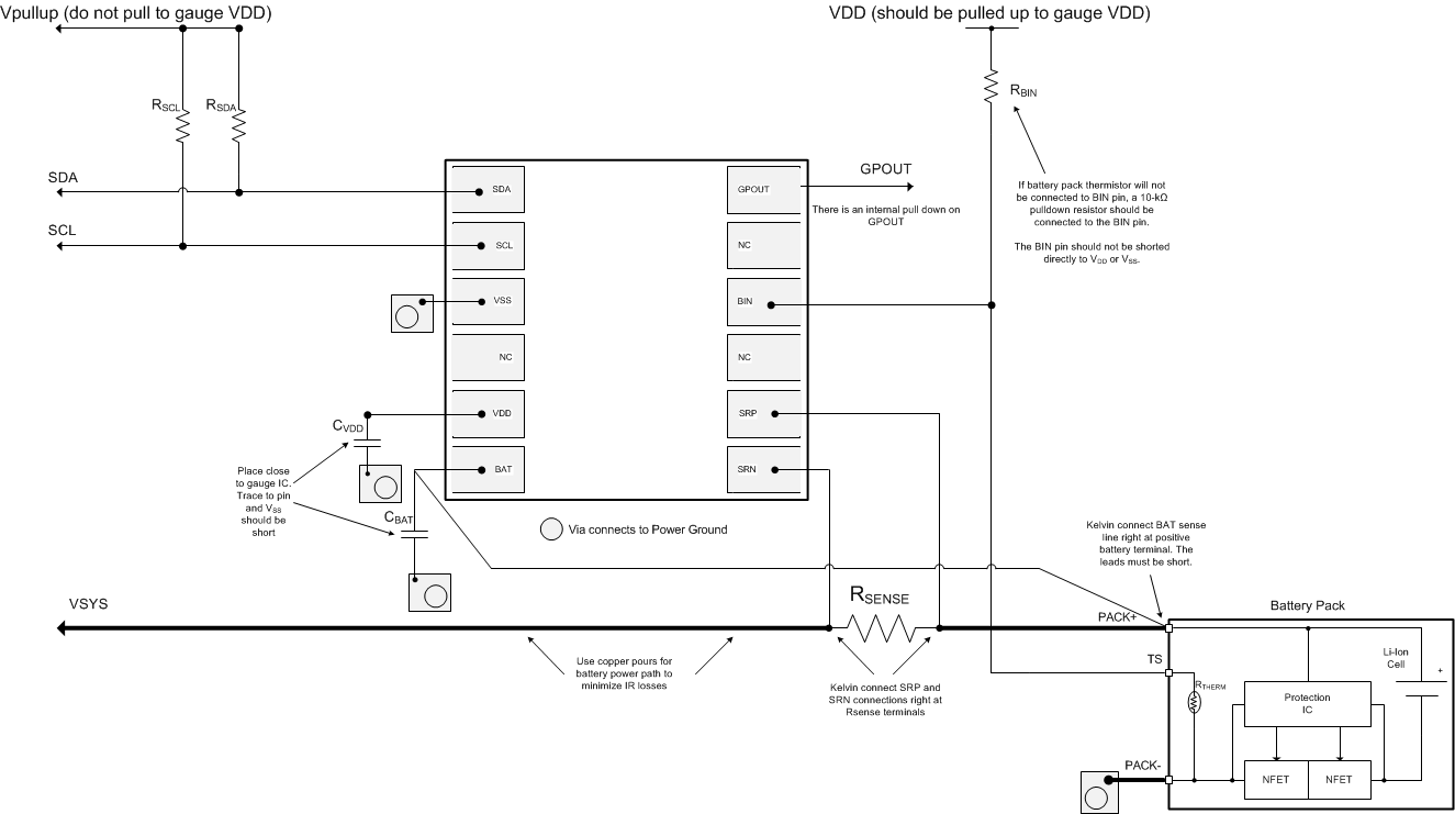
12 Layout
12.1 Layout Guidelines
- A capacitor of a value of at least 0.47 µF is connected between the VDD pin and VSS. The capacitor should be placed close to the gauge IC and have short traces to both the VDD pin and VSS.
- It is required to have a capacitor of at least 1.0 µF connect between the BAT pin and VSS if the connection between the battery pack and the gauge BAT pin has the potential to pick up noise. The capacitor should be placed close to the gauge IC and have short traces to both the VDD pin and VSS.
- If the external pullup resistors on the SCL and SDA lines will be disconnected from the host during low-power operation, it is recommend to use external 1-MΩ pulldown resistors to VSS to avoid floating inputs to the I2C engine.
- The value of the SCL and SDA pullup resistors should take into consideration the pullup voltage and the bus capacitance. Some recommended values, assuming a bus capacitance of 10 pF, can be seen in Table 4.
- If the GPOUT pin is not used by the host, the pin should still be pulled up to VDD with a 4.7-kΩ or 10-kΩ resistor.
- If the battery pack thermistor is not connected to the BIN pin, the BIN pin should be pulled down to VSS with a 10-kΩ resistor.
- The BIN pin should not be shorted directly to VDD or VSS.
- The actual device ground is pin 3 (VSS).
- The SRP and SRN pins should be Kelvin connected to the RSENSE terminals. SRP to the battery pack side of RSENSE and SRN to the system side of the RSENSE.
- Kelvin connect the BAT pin to the battery PACKP terminal.
Table 4. Recommended Values for SCL and SDA Pullup Resistors
| VPU | 1.8 V | 3.3 V | ||
|---|---|---|---|---|
| RPU | Range | Typical | Range | Typical |
| 400 Ω ≤ RPU ≤ 37.6 kΩ | 10 kΩ | 900 Ω ≤ RPU ≤ 29.2 kΩ | 5.1 kΩ | |