SLUSA52C September 2010 – March 2016
PRODUCTION DATA.
- 1 Features
- 2 Applications
- 3 Description
- 4 Revision History
- 5 Device Options
- 6 Pin Configuration and Functions
- 7 Specifications
- 8 Detailed Description
- 9 Application and Implementation
- 10Power Supply Recommendations
- 11Layout
- 12Device and Documentation Support
- 13Mechanical, Packaging, and Orderable Information
Package Options
Refer to the PDF data sheet for device specific package drawings
Mechanical Data (Package|Pins)
- DRB|8
Thermal pad, mechanical data (Package|Pins)
- DRB|8
Orderable Information
9 Application and Implementation
NOTE
Information in the following applications sections is not part of the TI component specification, and TI does not warrant its accuracy or completeness. TI’s customers are responsible for determining suitability of components for their purposes. Customers should validate and test their design implementation to confirm system functionality.
9.1 Application Information
The bq2920x is designed to be used in 2-series Li-Ion battery packs and with the option to include voltage-based cell balancing. The number of parallel cells or the overall capacity of the battery only affects the cell balancing circuit due to the level of potential imbalance that needs to be corrected.
9.2 Typical Applications
9.2.1 Battery Connection
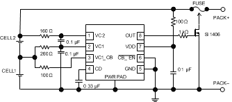
Figure 9 shows the configuration for the 2-series cell battery connection with cell balancing enabled.
 Figure 9. 2-Series Cell Configuration
9.2.1.1 Design Requirements
For this design example, use the parameters listed in Table 1.
Table 1. Design Parameters
| DESIGN PARAMETER | EXAMPLE VALUE at TA = 25°C |
|---|---|
| Input voltage range | 4 V to 10 V |
| Overvoltage Protection (OVT) | 4.35 V |
| Overvoltage detection delay time | 3 s |
| Overvoltage detection delay timer capacitor | 0.33 µF |
| Cell Balancing Enabled | Yes |
| Cell Balancing Current, ICB1 and ICB2 | 10 mA |
| Cell Balancing Resistors, RCB, RCB1, RCB2 and RVD | RCB = 100 Ω, RCB1 = 260 Ω, RCB2 = 160 Ω, RVD = 100 Ω |
9.2.1.2 Detailed Design Procedure
The bq2920x has limited features but there are some key calculations to be made when selecting external component values.
- Calculate the required CCD capacitor value for the voltage protection delay time. Care should be taken to evaluate the tolerances of the capacitor and the bq2920x to ensure system specifications are met.
- Calculate the cell balancing resistor values to provide a suitable level of balancing current that will, at a minimum, counter act an increase in imbalance during normal operation of the battery. Care should be taken to ensure any connectivity resistance is also considered as this will also reduce the balancing current level.
9.2.1.3 Application Curve
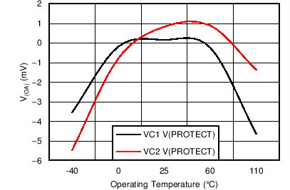
 Figure 10. Average VPROTECT Accuracy (VOA) Across Operation Temperature
9.3 System Example
9.3.1 External Cell Balancing
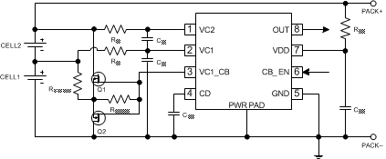
Higher cell balancing currents can be supported by means of a simple external network, as shown in Figure 11.
RCLAMP ensures that both Q1 and Q2 remain off when balancing is disabled, and should be sized above 2 kΩ to prevent excessive internal device current when the balancing network is activated. RCB_EXT determines the value of the balancing current, and is dependent on the voltage of the balanced cell, as follows:

