SLUSA52C September 2010 – March 2016
PRODUCTION DATA.
- 1 Features
- 2 Applications
- 3 Description
- 4 Revision History
- 5 Device Options
- 6 Pin Configuration and Functions
- 7 Specifications
- 8 Detailed Description
- 9 Application and Implementation
- 10Power Supply Recommendations
- 11Layout
- 12Device and Documentation Support
- 13Mechanical, Packaging, and Orderable Information
Package Options
Refer to the PDF data sheet for device specific package drawings
Mechanical Data (Package|Pins)
- DRB|8
Thermal pad, mechanical data (Package|Pins)
- DRB|8
Orderable Information
8 Detailed Description
8.1 Overview
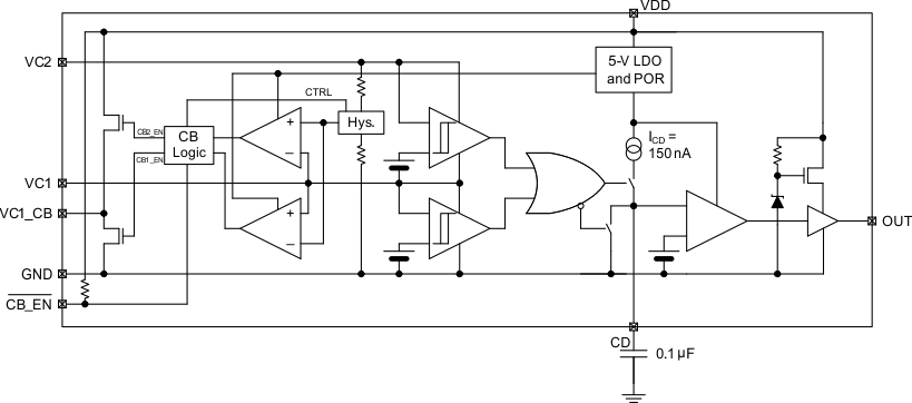
The bq2920x provides overvoltage protection and cell balancing for 2-series cell lithium-ion battery packs.
8.1.1 Voltage Protection
Each cell voltage is continuously compared to a factory configured internal reference threshold. If either cell reaches an overvoltage condition, the bq2920x device starts a timer that provides a delay proportional to the capacitance on the CD pin. Upon expiration of the internal timer, the OUT pin changes from a low to high state.
8.1.2 Cell Balancing
If enabled, the bq2920x performs automatic cell-balance correction where the two cells are automatically corrected for voltage imbalance by loading the cell with the higher voltage with a small balancing current. When the cells are measured to be equal within nominally 0 mV, the load current is removed. It will be re-applied if the imbalance exceeds nominally 30 mV. The cell mismatch correction circuitry is enabled by pulling the CB_EN pin low, and disabled when CB_EN is pulled to greater than 2.2 V, for example, VDD.
If the internal cell balancing current of up to 15 mA is insufficient, the bq2920x may be configured via external circuitry to support much higher external cell balancing current.
8.2 Functional Block Diagram
8.3 Feature Description
8.3.1 Protection (OUT) Timing
Sizing the external capacitor is based on the desired delay time as follows:

Where td is the desired delay time and XDELAY is the overvoltage delay time scale factor, expressed in seconds per microFarad. XDELAY is nominally 9 s/µF. For example, if a nominal delay of 3 seconds is desired, use a CCD capacitor that is 3 s / 9 s/µF = 0.33 µF.
The delay time is calculated as follows:

If the cell overvoltage condition is removed before the external capacitor reaches the reference voltage, the internal current source is disabled and an internal discharge block is employed to discharge the external capacitor down to 0 V. In this instance, the OUT pin remains in a low state.
8.3.2 Cell Voltage > VPROTECT
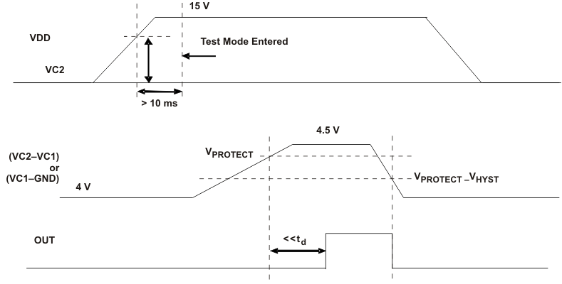
When one or both of the cell voltages rises above VPROTECT, the internal comparator is tripped, and the delay begins to count to td. If the input remains above VPROTECT for the duration of td, the bq2920x output changes from a low to a high state, by means of an internal pull-up network, to a regulated voltage of no more than 9.5 V when IOH = 0 mA.
The external delay capacitor should charge up to no more than the internal LDO voltage (approximately 5 V typically), and will fully discharge in approximately under 100 ms when the overvoltage condition is removed.
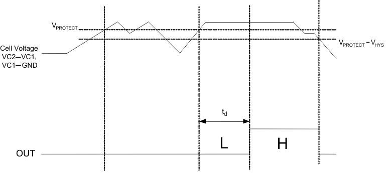 Figure 4. Timing for Overvoltage Sensing
8.3.3 Cell Connection Sequence
NOTE
Before connecting the cells, populate the overvoltage delay timing capacitor, CCD.
The recommended cell connection sequence begins from the bottom of the stack, as follows:
- GND
- VC1
- VC2
While not advised, connecting the cells in a sequence other than that described above does not result in errant activity on the OUT pin. For example:
- GND
- VC2 or VC1
- Remaining VCx pin
8.3.4 Cell Balance Enable Control
To avoid prematurely discharging the cells, it is recommended to turn off (pull high) the active-low Cell Balance Enable Control pin at lower State of Charge (SOC) levels.
8.3.5 Cell Balance Configuration
The cell balancing current may be calculated as follows:
For Cell 1 (VC1–GND) balancing current, ICB1:

For Cell 2 (VC2–VC1) balancing current, ICB2:

Where:
RCB = resistor connected between the top of Cell 1 and the VC1_CB
RCB1 = resistor connected between the top of Cell 1 and the VC1
RCB2 = resistor connected between the top of Cell 2 and the VC2
RVD = resistor connected between the top of Cell 2 and the VDD
8.3.6 Cell Imbalance Auto-Detection (Via Cell Voltage)
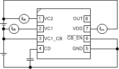
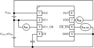
The VMM_DET_ON and VMM_DET_OFF specifications are calibrated where VDD = VC2 = 7.6 V and VC1 = 3.8 V. The recommended range of cell balancing is VC2 and VDD between 6.0 V and 8.4 V, and VC1 between 3 V and 4.2 V. Below VDD = 6 V, it is recommended to pull CB_EN high to disable the cell balancing function.
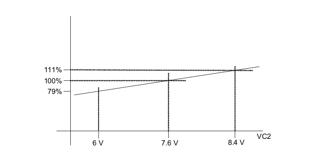 Figure 5. VMM_DET_ON and VMM_DET_OFF Threshold
8.3.7 Customer Test Mode
Customer Test Mode (CTM) helps to greatly reduce the overvoltage detection delay time and enable quicker customer production testing. This mode is intended for quick-pass board-level verification tests, and, as such, individual cell overvoltage levels may deviate slightly from the specifications (VPROTECT, VOA). If accurate overvoltage thresholds are to be tested, use the standard delay settings that are intended for normal use.
To enter CTM, VDD should be set to approximately 9.5 V higher than VC2. When CTM is entered, the device switches from the normal overvoltage delay time scale factor, XDELAY, to a significantly reduced factor of approximately 0.08, thereby reducing the delay time during an overvoltage condition.
CAUTION
Avoid exceeding any Absolute Maximum Voltages on any pins when placing the part into CTM. Also, avoid exceeding absolute maximum voltages for the individual cell voltages (VC1–GND) and (VC2–VC1). Stressing the pins beyond the rated limits may cause permanent damage to the device.
To exit CTM, power off the device and then power it back on.
8.4 Device Functional Modes
This device monitors the voltage of the cells connected to the VCx pins and depending on these voltages and the overall battery voltage at VDD the device enters different operating modes.
8.4.1 NORMAL Mode
The device is operating in NORMAL mode when the cell voltage range is between the over-charge detection threshold (VPROTECT) and the minimum supply voltage.
If this condition is satisfied, the device turns OFF the OUT pin.
8.4.2 PROTECTION Mode
The device is operating in PROTECTION mode when the cell over voltage protection feature has been triggered. See Cell Voltage > VPROTECT for more details on this feature.
If this condition is satisfied, the device turns ON the OUT pin.
