SLUSC67B March 2016 – October 2017
PRODUCTION DATA.
- 1 Features
- 2 Applications
- 3 Description
- 4 Revision History
- 5 Pin Configuration and Functions
-
6 Specifications
- 6.1 Absolute Maximum Ratings
- 6.2 ESD Ratings
- 6.3 Recommended Operating Conditions
- 6.4 Thermal Information
- 6.5 Electrical Characteristics: Supply Current
- 6.6 Electrical Characteristics: Power Supply Control
- 6.7 Electrical Characteristics: AFE Power-On Reset
- 6.8 Electrical Characteristics: AFE Watchdog Reset and Wake Timer
- 6.9 Electrical Characteristics: Current Wake Comparator
- 6.10 Electrical Characteristics: VC1, VC2, VC3, VC4, BAT, PACK
- 6.11 Electrical Characteristics: SMBD, SMBC
- 6.12 Electrical Characteristics: PRES, BTP_INT, DISP
- 6.13 Electrical Characteristics: LEDCNTLA, LEDCNTLB, LEDCNTLC
- 6.14 Electrical Characteristics: Coulomb Counter
- 6.15 Electrical Characteristics: CC Digital Filter
- 6.16 Electrical Characteristics: ADC
- 6.17 Electrical Characteristics: ADC Digital Filter
- 6.18 Electrical Characteristics: CHG, DSG FET Drive
- 6.19 Electrical Characteristics: PCHG FET Drive
- 6.20 Electrical Characteristics: FUSE Drive
- 6.21 Electrical Characteristics: Internal Temperature Sensor
- 6.22 Electrical Characteristics: TS1, TS2, TS3, TS4
- 6.23 Electrical Characteristics: PTC, PTCEN
- 6.24 Electrical Characteristics: Internal 1.8-V LDO
- 6.25 Electrical Characteristics: High-Frequency Oscillator
- 6.26 Electrical Characteristics: Low-Frequency Oscillator
- 6.27 Electrical Characteristics: Voltage Reference 1
- 6.28 Electrical Characteristics: Voltage Reference 2
- 6.29 Electrical Characteristics: Instruction Flash
- 6.30 Electrical Characteristics: Data Flash
- 6.31 Electrical Characteristics: OCD, SCC, SCD1, SCD2 Current Protection Thresholds
- 6.32 Timing Requirements: OCD, SCC, SCD1, SCD2 Current Protection Timing
- 6.33 Timing Requirements: SMBus
- 6.34 Timing Requirements: SMBus XL
- 6.35 Typical Characteristics
-
7 Detailed Description
- 7.1 Overview
- 7.2 Functional Block Diagram
- 7.3
Feature Description
- 7.3.1 Primary (1st Level) Safety Features
- 7.3.2 Secondary (2nd Level) Safety Features
- 7.3.3 Charge Control Features
- 7.3.4 Gas Gauging
- 7.3.5 Configuration
- 7.3.6 Battery Parameter Measurements
- 7.3.7 Battery Trip Point (BTP)
- 7.3.8 Lifetime Data Logging Features
- 7.3.9 Authentication
- 7.3.10 LED Display
- 7.3.11 Voltage
- 7.3.12 Current
- 7.3.13 Temperature
- 7.3.14 Communications
- 7.4 Device Functional Modes
- 8 Applications and Implementation
- 9 Power Supply Recommendations
- 10Layout
- 11Device and Documentation Support
- 12Mechanical, Packaging, and Orderable Information
Package Options
Mechanical Data (Package|Pins)
- RSM|32
Thermal pad, mechanical data (Package|Pins)
- RSM|32
Orderable Information
8 Applications and Implementation
NOTE
Information in the following applications sections is not part of the TI component specification, and TI does not warrant its accuracy or completeness. TI’s customers are responsible for determining suitability of components for their purposes. Customers should validate and test their design implementation to confirm system functionality.
8.1 Application Information
The bq4050 gas gauge has primary protection support to be used with a 1-series to 4-series Li-Ion/Li Polymer battery pack. To implement and design a comprehensive set of parameters for a specific battery pack, users need the Battery Management Studio (bqStudio) graphical user-interface tool installed on a PC during development. The firmware installed on the bqStudio tool has default values for this product, which are summarized in the bq4050 Technical Reference Manual (SLUUAQ3). Using the bqStudio tool, these default values can be changed to cater to specific application requirements during development once the system parameters, such as fault trigger thresholds for protection, enable/disable of certain features for operation, configuration of cells, chemistry that best matches the cell used, and more are known. This data is referred to as the "golden image."
8.2 Typical Applications
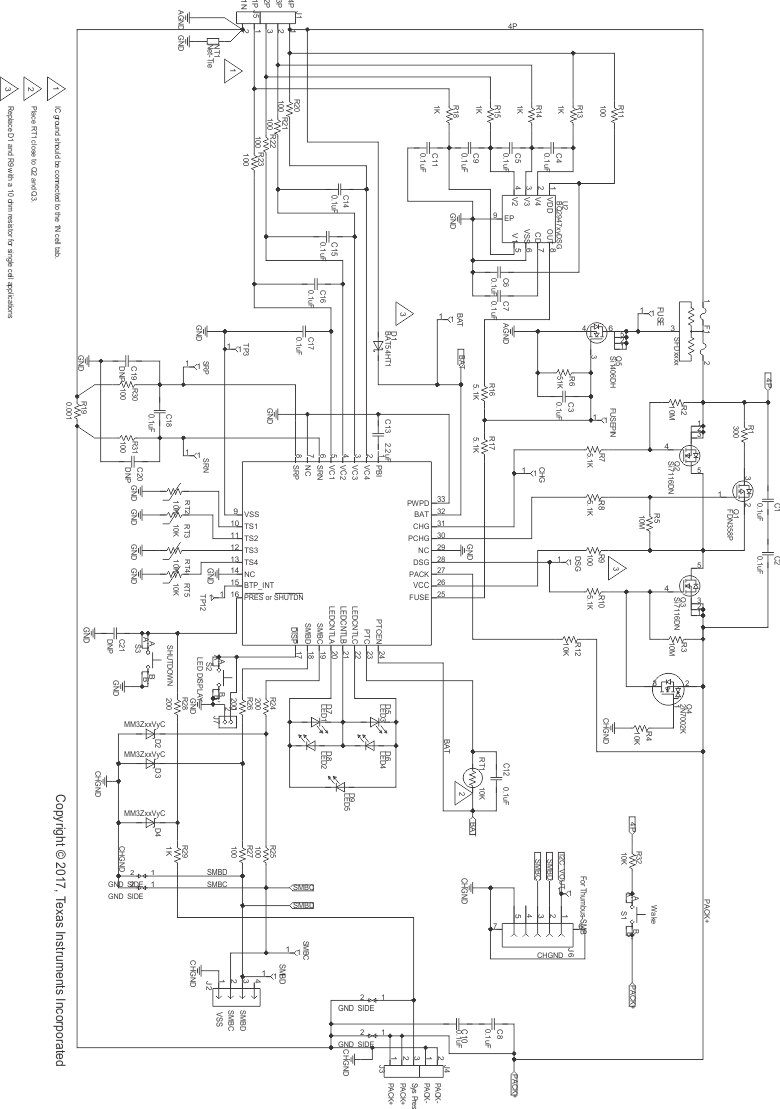 Figure 21. Application Schematic
8.2.1 Design Requirements
Table 1 shows the default settings for the main parameters. Use the bqStudio tool to update the settings to meet the specific application or battery pack configuration requirements.
The device should be calibrated before any gauging test. Follow the information in the bqStudio Calibration page to calibrate the device, and use the bqStudio Chemistry page to update the match chemistry profile to the device.
Table 1. Design Parameters
| DESIGN PARAMETER | EXAMPLE |
|---|---|
| Cell Configuration | 3s1p (3-series with 1 Parallel)(1) |
| Design Capacity | 4400 mAh |
| Device Chemistry | 1210 (LiCoO2/graphitized carbon) |
| Cell Overvoltage at Standard Temperature | 4300 mV |
| Cell Undervoltage | 2500 mV |
| Shutdown Voltage | 2300 mV |
| Overcurrent in CHARGE Mode | 6000 mA |
| Overcurrent in DISCHARGE Mode | –6000 mA |
| Short Circuit in CHARGE Mode | 0.1 V/Rsense across SRP, SRN |
| Short Circuit in DISCHARGE Mode | 0.1 V/Rsense across SRP, SRN |
| Safety Overvoltage | 4500 mV |
| Cell Balancing | Disabled |
| Internal and External Temperature Sensor | External Temperature Sensors are used. |
| Undertemperature Charging | 0°C |
| Undertemperature Discharging | 0°C |
| BROADCAST Mode | Disabled |
| Battery Trip Point (BTP) with active high interrupt | Disabled |
8.2.2 Detailed Design Procedure
8.2.2.1 High-Current Path
The high-current path begins at the PACK+ terminal of the battery pack. As charge current travels through the pack, it finds its way through protection FETs, a chemical fuse, the lithium-ion cells and cell connections, and the sense resistor, and then returns to the PACK– terminal (see Figure 22). In addition, some components are placed across the PACK+ and PACK– terminals to reduce effects from electrostatic discharge.
8.2.2.1.1 Protection FETs
Select the N-CH charge and discharge FETs for a given application. Most portable battery applications are a good match for the CSD17308Q3. The TI CSD17308Q3 is a 47A, 30-V device with Rds(on) of 8.2 mΩ when the gate drive voltage is 8 V.
If a precharge FET is used, R1 is calculated to limit the precharge current to the desired rate. Be sure to account for the power dissipation of the series resistor. The precharge current is limited to (VCHARGER – VBAT)/R1 and maximum power dissipation is (Vcharger – Vbat)2/R1.
The gates of all protection FETs are pulled to the source with a high-value resistor between the gate and source to ensure they are turned off if the gate drive is open.
Capacitors C1 and C2 help protect the FETs during an ESD event. Using two devices ensures normal operation if one becomes shorted. To have good ESD protection, the copper trace inductance of the capacitor leads must be designed to be as short and wide as possible. Ensure that the voltage ratings of C1 and C2 are adequate to hold off the applied voltage if one of the capacitors becomes shorted.
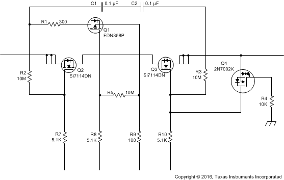 Figure 22. bq4050 Protection FETs
8.2.2.1.2 Chemical Fuse
The chemical fuse (Dexerials, Uchihashi, and so on) is ignited under command from either the bq294700 secondary voltage protection IC or from the FUSE pin of the gas gauge. Either of these events applies a positive voltage to the gate of Q5, shown in Figure 23, which then sinks current from the third terminal of the fuse, causing it to ignite and open permanently.
It is important to carefully review the fuse specifications and match the required ignition current to that available from the N-CH FET. Ensure that the proper voltage, current, and Rds(on) ratings are used for this device. The fuse control circuit is discussed in detail in FUSE Circuitry.
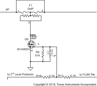 Figure 23. FUSE Circuit
8.2.2.1.3 Lithium-Ion Cell Connections
The important part to remember about the cell connections is that high current flows through the top and bottom connections; therefore, the voltage sense leads at these points must be made with a Kelvin connection to avoid any errors due to a drop in the high-current copper trace. The location marked 4P in Figure 24 indicates the Kelvin connection of the most positive battery node. The connection marked 1N is equally important. The VC5 pin (a ground reference for cell voltage measurement), which is in the older generation devices, is not in the bq4050 device. Therefore, the single-point connection at 1N to the low-current ground is needed to avoid an undesired voltage drop through long traces while the gas gauge is measuring the bottom cell voltage.
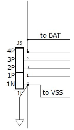 Figure 24. Lithium-Ion Cell Connections
8.2.2.1.4 Sense Resistor
As with the cell connections, the quality of the Kelvin connections at the sense resistor is critical. The sense resistor must have a temperature coefficient no greater than 50 ppm in order to minimize current measurement drift with temperature. Choose the value of the sense resistor to correspond to the available overcurrent and short-circuit ranges of the bq4050 gauge. Select the smallest value possible to minimize the negative voltage generated on the bq4050 VSS node(s) during a short circuit. This pin has an absolute minimum of –0.3 V. Parallel resistors can be used as long as good Kelvin sensing is ensured. The device is designed to support a 1-mΩ to 3-mΩ sense resistor.
The ground scheme of bq4050 gauge is different from the older generation devices. In previous devices, the device ground (or low current ground) is connected to the SRN side of the Rsense resistor pad. The bq4050 gauge, however, it connects the low-current ground on the SRP side of the Rsense resistor pad close to the battery 1N terminal (see Lithium-Ion Cell Connections). This is because the bq4050 gauge has one less VC pin (a ground reference pin VC5) compared to the previous devices. The pin was removed and was internally combined to SRP.
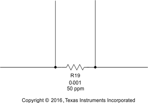 Figure 25. Sense Resistor
8.2.2.1.5 ESD Mitigation
A pair of series 0.1-μF ceramic capacitors is placed across the PACK+ and PACK– terminals to help in the mitigation of external electrostatic discharges. The two devices in series ensure continued operation of the pack if one of the capacitors becomes shorted.
Optionally, a tranzorb such as the SMBJ2A can be placed across the terminals to further improve ESD immunity.
8.2.2.2 Gas Gauge Circuit
The gas gauge circuit includes the bq4050 gauge and its peripheral components. These components are divided into the following groups: Differential Low-Pass Filter, PBI, system present, SMBus Communication, FUSE circuit, and LED.
8.2.2.2.1 Coulomb-Counting Interface
The bq4050 gauge uses an integrating delta-sigma ADC for current measurements. Add a 100-Ω resistor from the sense resistor to the SRP and SRN inputs of the device. Place a 0.1-µF (C18) filter capacitor across the SRP and SRN inputs. Optional 0.1-µF filter capacitors (C19 and C20) can be added for additional noise filtering if required for a circuit.
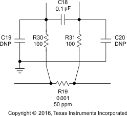 Figure 26. Differential Filter
8.2.2.2.2 Power Supply Decoupling and PBI
The bq4050 gauge has an internal LDO that is internally compensated and does not require an external decoupling capacitor.
The PBI pin is used as a power supply backup input pin providing power during brief transient power outages. A standard 2.2-µF ceramic capacitor is connected from the PBI pin to ground as shown in Figure 27.
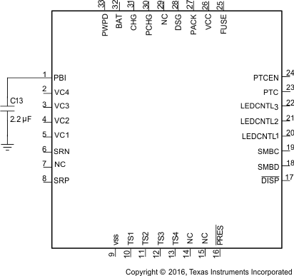 Figure 27. Power Supply Decoupling
8.2.2.2.3 System Present
The system present signal is used to inform the gas gauge whether the pack is installed into or removed from the system. In the host system, this pin is grounded. The PRES pin of the bq4050 gauge is occasionally sampled to test for system present. To save power, an internal pullup is provided by the gas gauge during a brief 4-μs sampling pulse once per second. A resistor can be used to pull the signal low and the resistance must be 20 kΩ or lower to ensure that the test pulse is lower than the VIL limit. The pullup current source is typically 10 µA to 20 µA.
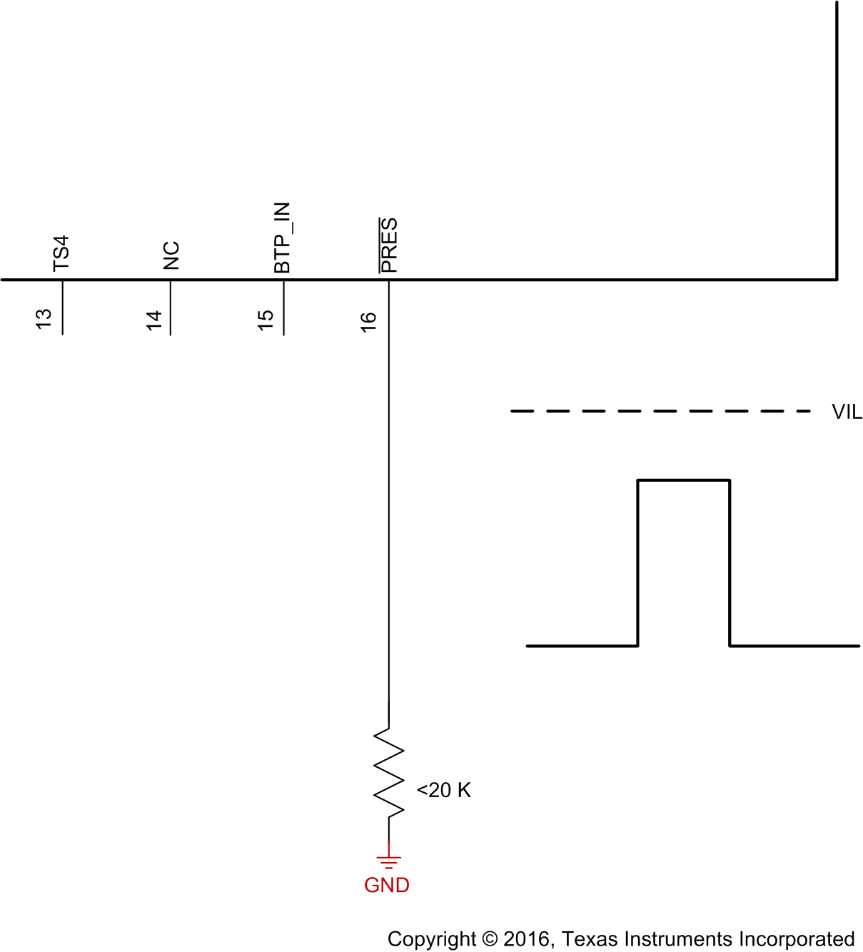 Figure 28. System Present Pull-Down Resistor
Because the system present signal is part of the pack connector interface to the outside world, it must be protected from external electrostatic discharge events. An integrated ESD protection on the PRES device pin reduces the external protection requirement to just R29 for an 8-kV ESD contact rating. However, if it is possible that the system present signal may short to PACK+, then R28 and D4 must be included for high-voltage protection.
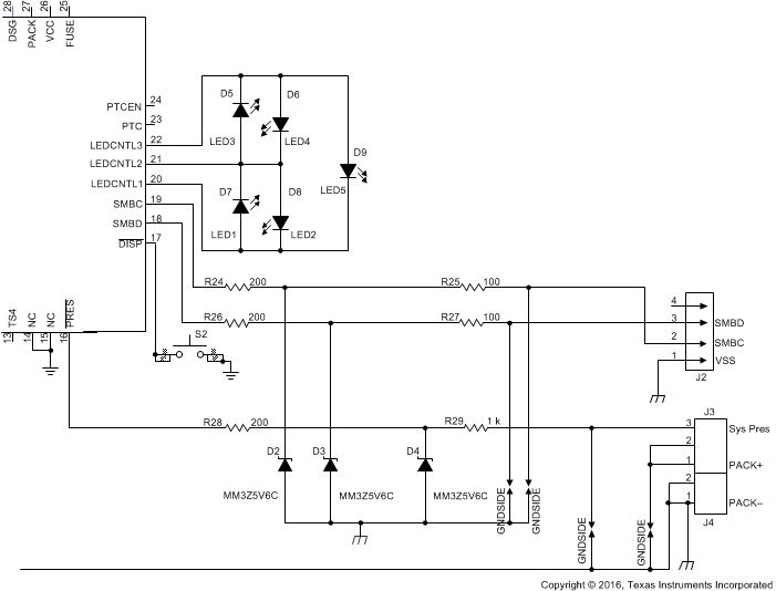 Figure 29. System Present ESD and Short Protection
8.2.2.2.4 SMBus Communication
The SMBus clock and data pins have integrated high-voltage ESD protection circuits; however, adding a Zener diode (D2 and D3) and series resistor (R24 and R26) provides more robust ESD performance.
The SMBus clock and data lines have internal pulldown. When the gas gauge senses that both lines are low (such as during removal of the pack), the device performs auto-offset calibration and then goes into SLEEP mode to conserve power.
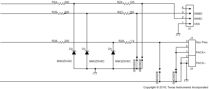 Figure 30. ESD Protection for SMB Communication
8.2.2.2.5 FUSE Circuitry
The FUSE pin of the bq4050 gauge is designed to ignite the chemical fuse if one of the various safety criteria is violated. The FUSE pin also monitors the state of the secondary-voltage protection IC. Q5 ignites the chemical fuse when its gate is high. The 7-V output of the bq294700 is divided by R16 and R6, which provides adequate gate drive for Q5 while guarding against excessive back current into the bq294700 if the FUSE signal is high.
Using C3 is generally a good practice, especially for RFI immunity. C3 may be removed, if desired, because the chemical fuse is a comparatively slow device and is not affected by any submicrosecond glitches that come from the FUSE output during the cell connection process.
 Figure 31. FUSE Circuit
When the bq4050 gauge is commanded to ignite the chemical fuse, the FUSE pin activates to give a typical 8-V output. The new design makes it possible to use a higher Vgs FET for Q5. This improves the robustness of the system, as well as widens the choices for Q5.
8.2.2.3 Secondary-Current Protection
The bq4050 gauge provides secondary overcurrent and short-circuit protection, cell balancing, cell voltage multiplexing, and voltage translation. The following discussion examines cell and battery inputs, pack and FET control, temperature output, and cell balancing.
8.2.2.3.1 Cell and Battery Inputs
Each cell input is conditioned with a simple RC filter, which provides ESD protection during cell connect and acts to filter unwanted voltage transients. The resistor value allows some trade-off for cell balancing versus safety protection.
The integrated cell balancing FETs allow the AFE to bypass cell current around a given cell or numerous cells, effectively balancing the entire battery stack. External series resistors placed between the cell connections and the VCx I/O pins set the balancing current magnitude. The internal FETs provide a 200-Ω resistance (2 V < VDS < 4 V). Series input resistors between 100 Ω and 1 kΩ are recommended for effective cell balancing.
The BAT input uses a diode (D1) to isolate and decouple it from the cells in the event of a transient dip in voltage caused by a short-circuit event.
Also, as described in High-Current Path, the top and bottom nodes of the cells must be sensed at the battery connections with a Kelvin connection to prevent voltage sensing errors caused by a drop in the high-current PCB copper.
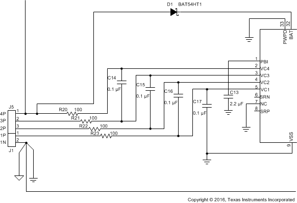 Figure 32. Cell and BAT Inputs
8.2.2.3.2 External Cell Balancing
Internal cell balancing can only support up to 10 mA. External cell balancing is provided as another option for faster cell balancing. For details, refer to the application note, Fast Cell Balancing Using External MOSFET (SLUA420).
8.2.2.3.3 PACK and FET Control
The PACK and VCC inputs provide power to the bq4050 gauge from the charger. The PACK input also provides a method to measure and detect the presence of a charger. The PACK input uses a 100-Ω resistor; whereas, the VCC input uses a diode to guard against input transients and prevents misoperation of the date driver during short-circuit events.
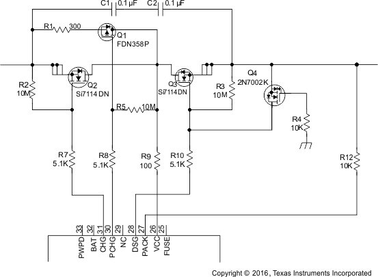 Figure 33. bq4050 PACK and FET Control
The N-CH charge and discharge FETs are controlled with 5.1-kΩ series gate resistors, which provide a switching time constant of a few microseconds. The 10-MΩ resistors ensure that the FETs are off in the event of an open connection to the FET drivers. Q4 is provided to protect the discharge FET (Q3) in the event of a reverse-connected charger. Without Q4, Q3 can be driven into its linear region and suffer severe damage if the PACK+ input becomes slightly negative.
Q4 turns on in that case to protect Q3 by shorting its gate to source. To use the simple ground gate circuit, the FET must have a low gate turn-on threshold. If it is desired to use a more standard device, such as the 2N7002 as the reference schematic, the gate should be biased up to 3.3 V with a high-value resistor. The bq4050 device has the capability to provide a current-limited charging path typically used for low battery voltage or low temperature charging. The bq4050 device uses an external P-channel, precharge FET controlled by PCHG.
8.2.2.3.4 Temperature Output
For the bq4050 device, TS1, TS2, TS3, and TS4 provide thermistor drive-under program control. Each pin can be enabled with an integrated 18-kΩ (typical) linearization pullup resistor to support the use of a 10-kΩ at 25°C (103) NTC external thermistor, such as a Mitsubishi BN35-3H103. The reference design includes four 10-kΩ thermistors: RT1, RT2, RT3, and RT4. The bq4050 device supports up to four external thermistors. Connect unused thermistor pins to VSS.
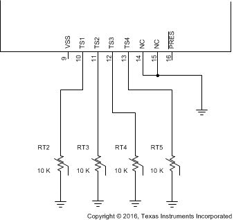 Figure 34. Thermistor Drive
8.2.2.3.5 LEDs
Three LED control outputs provide constant current sinks for the driving external LEDs. These outputs are configured to provide voltage and control for up to 5 LEDs. No external bias voltage is required. Unused LEDCNTL pins can remain open or they can be connected to VSS. The DISP pin should be connected to VSS, if the LED feature is not used.
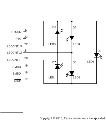 Figure 35. LEDs
8.2.2.3.6 Safety PTC Thermistor
The bq4050 device provides support for a safety PTC thermistor. The PTC thermistor is connected between PTC and PTCEN, and PTCEN is connected to BAT. It can be placed close to the CHG/DSG FETs to monitor the temperature. A PTC fault is one of the permanent failure modes. It can only be cleared by a POR.
To disable, connect PTC and PTCEN to VSS.
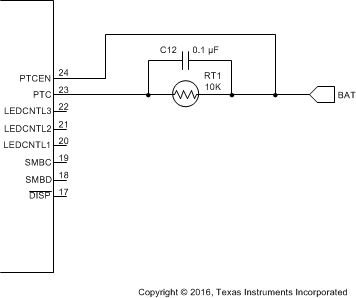 Figure 36. PTC Thermistor
8.2.3 Application Curves
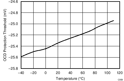
| Threshold setting is –25 mV. | ||
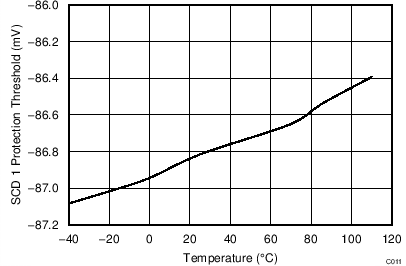
| Threshold setting is –88.85 mV. | ||
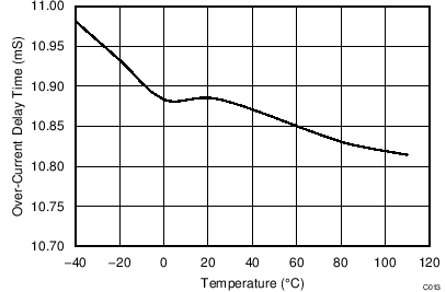
| Threshold setting is 11 ms. | ||
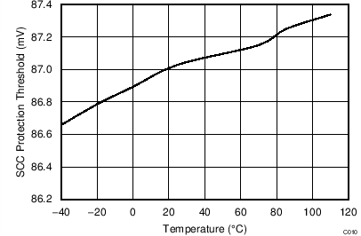
| Threshold setting is 88.85 mV. | ||
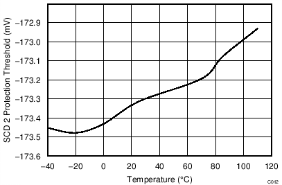
| Threshold setting is –177.7 mV. | ||
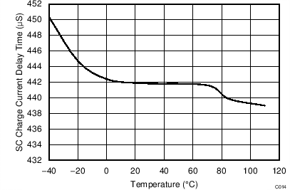
| Threshold setting is 465 µs. | ||