SLUSAW3D December 2014 – January 2017
PRODUCTION DATA.
- 1 Features
- 2 Applications
- 3 Description
- 4 Revision History
- 5 Description (continued)
- 6 Pin Configuration and Functions
-
7 Specifications
- 7.1 Absolute Maximum Ratings
- 7.2 ESD Ratings
- 7.3 Recommended Operating Conditions
- 7.4 Thermal Information
- 7.5 Supply Voltage
- 7.6 Supply Current
- 7.7 Power Supply Control
- 7.8 Low-Voltage General Purpose I/O (TSx)
- 7.9 High-Voltage General Purpose I/O (GPIO0, GPIO1)
- 7.10 AFE Power-On Reset
- 7.11 Internal 1.8-V LDO
- 7.12 Current Wake Comparator
- 7.13 Coulomb Counter
- 7.14 CC Digital Filter
- 7.15 ADC
- 7.16 ADC Digital Filter
- 7.17 ADC Multiplexer
- 7.18 Cell Balancing Support
- 7.19 Cell Detach Detection
- 7.20 Internal Temperature Sensor
- 7.21 NTC Thermistor Measurement Support (ADCx)
- 7.22 High-Frequency Oscillator
- 7.23 Low-Frequency Oscillator
- 7.24 Voltage Reference 1
- 7.25 Voltage Reference 2
- 7.26 Instruction Flash
- 7.27 Data Flash
- 7.28 Current Protection Thresholds
- 7.29 N-CH FET Drive (CHG, DSG)
- 7.30 FUSE Drive (AFEFUSE)
- 7.31 Battery Charger Voltage Regulation (VFB)
- 7.32 Battery Charger Current Sense (HSRP, HSRN)
- 7.33 Battery Charger Precharge Current Sense (HSRP, HSRN)
- 7.34 AC Adapter Fault Detect (HSRN, VCC)
- 7.35 Battery Charger Overcurrent Detection (V)HSRP, (V)HSRN
- 7.36 Battery Charger Undercurrent Detection (V)HSRP, (V)HSRN
- 7.37 System Operation Detection (V)HSRN
- 7.38 Battery Overvoltage Comparator (VFB)
- 7.39 Regulator (REGN)
- 7.40 PWM High-Side Driver (HiDRV)
- 7.41 PWM Low-Side Driver (LoDRV)
- 7.42 PWM Information
- 7.43 Charger Power-Up Sequence
- 7.44 Thermal Shutdown Comparator
- 7.45 SMBus High Voltage I/O
- 7.46 SMBus
- 7.47 SMBus XL
- 7.48 Timing Requirements
- 7.49 Typical Characteristics
-
8 Detailed Description
- 8.1 Overview
- 8.2 Functional Block Diagram
- 8.3 Feature Description
- 9 Application and Implementation
- 10Power Supply Recommendations
- 11Layout
- 12Device and Documentation Support
- 13Mechanical, Packaging, and Orderable Information
Package Options
Mechanical Data (Package|Pins)
- RHB|32
Thermal pad, mechanical data (Package|Pins)
- RHB|32
Orderable Information
11 Layout
11.1 Layout Guidelines
The following information is related to external component selection and guidelines for PCB layout.
11.1.1 PCB Layout
The switching node rise and fall times should be minimized for minimum switching loss. Proper layout of the components to minimize high-frequency current-path loop (see Figure 12) is important to prevent electrical and magnetic field radiation and high-frequency resonant problems. The following is a PCB layout priority list for proper layout. Layout of the PCB according to this specific order is essential.
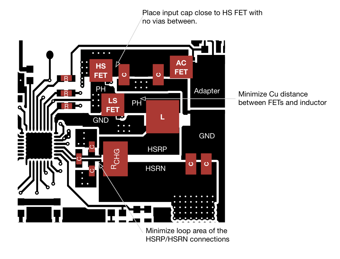
- Place the input capacitor as close as possible to the switching MOSFET supply and ground connections and use the shortest possible copper trace connection. The capacitors should be placed on the same layer as the FETs instead of using vias to connect the capacitor and the FETs. Additionally, any vias connecting the input capacitor to the adaptor node should not be placed between the capacitor and the FETs; the capacitor should have a solid copper path to the FET.
- The IC should be placed close to the switching MOSFET gate pins to keep the gate-drive signal traces short for a clean MOSFET drive. The IC can be placed on the other side of the PCB from the switching MOSFETs.
- Place the inductor input pin as close as possible to the switching MOSFET output pin. Minimize the copper area of this trace to lower electrical and magnetic field radiation, but make the trace wide enough to carry the charging current. Do not use multiple layers in parallel for this connection. Minimize parasitic capacitance from this area to any other trace or plane.
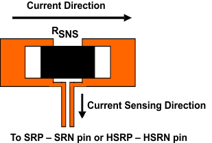
- The charging-current sensing resistor should be placed right next to the inductor output. Route the sense leads connected across the sensing resistor back to the IC in same layer, close to each other (minimize loop area) and do not route the sense leads through a high-current path (see Figure 13 for Kelvin connection for best current accuracy). Place the decoupling capacitor on these traces next to the IC.
- Place the output capacitor next to the sensing resistor output and ground.
- Output capacitor ground connections must be tied to the same copper that connects to the input capacitor ground before connecting to system ground.
- Place the sense resistor and filter components, R1, C2, and C3, as close as possible to the IC and directly adjacent to the decoupling capacitor between HSRN and HSRP.
- Route the analog ground separately from the power ground and use a single ground connection to tie the charger power ground to the charger analog ground. Just beneath the IC, use the copper-pour for analog ground, but avoid power pins to reduce inductive and capacitive noise coupling. Connect analog ground to GND. Connect analog ground and power ground together using the thermal pad as the single ground connection point. Or use a 0-Ω resistor to tie analog ground to power ground (thermal pad should tie to analog ground in this case). A star connection under the thermal pad is highly recommended.
- It is critical that the exposed thermal pad on the back side of the IC package be soldered to the PCB ground. Ensure that there are sufficient thermal vias directly under the IC connecting to the ground plane on the other layers.
- Place decoupling capacitors next to the IC pins and make the trace connection as short as possible.
- Size and number of all vias should be enough for a given current path.
 Figure 12. High-Frequency Current Path
 Figure 13. Sensing Resistor PCB Layout
For the recommended component placement with trace and via locations, see the bq40z60EVM SBS 1.1 Impedance Track™ Technology Enabled Battery Management Solution Evaluation Module User's Guide (SLUUB71).
For the QFN information, see the Quad Flatpack No-Lead Logic Packages Application Note (SCBA017) and the QFN/SON PCB Attachment Application Note (SLUA271).
11.2 Layout Example
 Figure 14. Board Layout Example