SLUSBD6D July 2013 – July 2016
PRODUCTION DATA.
- 1 Features
- 2 Applications
- 3 Description
- 4 Revision History
- 5 Pin Configuration and Functions
- 6 Specifications
-
7 Detailed Description
- 7.1 Overview
- 7.2 Functional Block Diagram
- 7.3 Feature Description
- 7.4 Device Functional Modes
- 7.5 Programming
- 8 Application and Implementation
- 9 Power Supply Recommendations
- 10Layout
- 11Device and Documentation Support
- 12Mechanical, Packaging, and Orderable Information
Package Options
Mechanical Data (Package|Pins)
- RGZ|48
Thermal pad, mechanical data (Package|Pins)
- RGZ|48
Orderable Information
8 Application and Implementation
NOTE
Information in the following applications sections is not part of the TI component specification, and TI does not warrant its accuracy or completeness. TI s customers are responsible for determining suitability of components for their purposes. Customers should validate and test their design implementation to confirm system functionality.
8.1 Application Information
The bq500212A device is a wireless power transmitter controller designed for 5-W WPC compliant applications. The device has has all features required to support receivers that are compliant with WPC 1.0, 1.1, and Low Power 1.2. Additional tools and application information can be found in the bq500212A product folder. The following section highlight some of the system design considerations.
8.2 Typical Application
Figure 9 shows the application schematic for the transmitted with reduced standby power.
NOTE
Check the bq500212A product page for the most up-to-date application schematic and list of materials package before starting a new design.
8.2.1 Design Requirements
For this design example, use the parameters listed in Table 3 as the input parameters.
Table 3. Design Parameters
| PARAMETER | EXAMPLE VALUE |
|---|---|
| WPC coil type | A11 and A5 |
| Input voltage | 5 V ±5% (5-V input to A11 / A5 TX) |
8.2.2 Detailed Design Procedure
8.2.2.1 PMOD, FOD, and FOD Calibration
The bq500212A device supports improved FOD (WPC1.1) and enhanced PMOD (WPC 1.0) features. Continuously monitoring input power, known losses, and the value of power reported by the RX device being charged, the bq500212A device can estimate how much power is unaccounted for and presumed lost due to metal objects placed in the wireless power transfer path. If this unexpected loss exceeds the threshold set by the FOD or PMOD resistors, a fault is indicated and power transfer is halted. Whether the FOD or the PMOD algorithm is used is determined by the ID packet of the receiver being charged.
As the default, both PMOD and FOD resistors must set a threshold of 400 mW (selected by 56.2-kΩ resistors from FOD and PMOD to LOSS_THR. 400 mW has been empirically determined using standard WPC FOD test objects (disc, ring, and foil). Some tuning might be required as every system is slightly different. This tuning is best done by trial and error, use the set resistor values given in the table to increase or decrease the loss threshold and retry the system with the standard test objects. The ultimate goal of the FOD feature is safety; to protect misplaced metal objects from becoming hot. Reducing the loss threshold and making the system too sensitive leads to false trips and a bad user experience. Find the balance which best suits the application.
If the application requires disabling one function or the other (or both), it is possible by leaving the respective FOD pin and PMOD pin open. For example, to selectively disable the PMOD function, PMOD must be left open.
NOTE
Disabling FOD results in a TX solution that is not WPC compliant.
Resistors of 1% tolerance must be used for a reliable selection of the desired threshold.
The FOD and PMOD resistors program the permitted power loss for the FOD and PMOD algorithms respectively. The FOD_CAL resistor, can be used to compensate for any load dependent effect on the power loss. Using a calibrated test receiver with no foreign objects present, the FOD_CAL resistor must be selected such that the calculated loss across the load range is substantially constant (within approximately 100 mW). After correcting for the load dependence, the FOD and PMOD thresholds must be reset above the resulting average by approximately 400 mW for the transmitter to satisfy the WPC requirements on tolerated heating. Contact TI for more information about setting appropriate FOD, PMOD, and FOD_CAL resistor values for your design.
Table 4. Option Select Bins
| BIN NUMBER | RESISTANCE (kΩ) | LOSS THRESHOLD (mW) |
|---|---|---|
| 0 | <36.5 | 250 |
| 1 | 42.2 | 300 |
| 2 | 48.7 | 350 |
| 3 | 56.2 | 400 |
| 4 | 64.9 | 450 |
| 5 | 75 | 500 |
| 6 | 86.6 | 550 |
| 7 | 100 | 600 |
| 8 | 115 | 650 |
| 9 | 133 | 700 |
| 10 | 154 | 750 |
| 11 | 178 | 800 |
| 12 | 205 | 850 |
| 13 | >237 | Feature Disabled |
8.2.2.2 Coils and Matching Capacitors
The coil and matching capacitor selection for the transmitter has been established by WPC standard. These values are fixed and cannot be changed on the transmitter side.
An up to date list of available and compatible A5 or A11 transmitter coils can be found in bqTESLA Transmitter Coil Vendors (SLUA649):
Capacitor selection is critical to proper system operation. A total capacitance value of 400 nF is required in the resonant tank. A 400-nF capacitor is not a standard value and therefore several must be combined in parallel. TI recommends to use 4 × 100 nF, as these are very commonly available.
NOTE
A total capacitance value of 400 nF/50 V is required in the resonant tank to achieve a 100-kHz resonance frequency.
To achieve the 400-nF total capacitance in the resonant tank, the bq500212A device sensitive demodulation circuitry allows the use of 3 lower cost 100-nF/X7R type capacitors in parallel with one (1) high quality 100-nF/C0G type, thereby reducing system cost from competitive solutions requiring four C0G types.
The capacitors chosen must be rated for 50 V operation. Use quality capacitors from reputable vendors such as KEMET, MURATA or TDK.
8.2.2.3 Design Checklist for WPC1.1 Compliance With the bq500212A
- Coil and capacitor selection matches the A5/A11 specification.
- Total 400-nF resonant capacitor requirement is composed of: (3 × 100nF/X7R) + (1 × 100nF/C0G) types.
- Precision current sense amp used, such as the INA199A1. This is required for accurate FOD operation.
- Current shunt resistor 1% and <200 PPM. This is required for accurate FOD operation.
8.2.2.4 Input Regulator
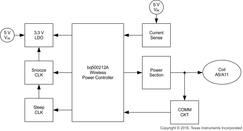
The bq500212A device requires 3.3 VDC to operate. A buck regulator or a linear regulator can be used to step down from the 5-V system input. Either choice is fully WPC compatible, the decision lies in the user's requirements with respect to cost or efficiency.
For lowest cost, TI recommends the TLV70033 linear regulator.
8.2.2.5 Power Train
The bq500212A device drives a phase-shifted full bridge. This is essentially twin half bridges and the choice of driver devices is quite simple; a pair of CSD97376 Integrated Power Stages are used. Other combinations using discrete driver and MOSFETs can work and system performance with regards to efficiency and EMI emissions vary. Any alternate MOSFETs chosen must be fully saturated at the 5-V system gate drive voltage available and be sure to pay attention whether or not to use gate resistors; some tuning might be required.
8.2.3 Application Curves
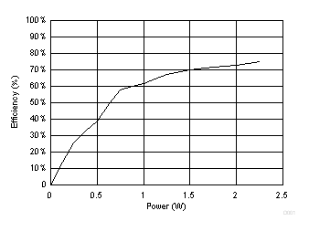
 Figure 10. Efficiency vs Power bq51003
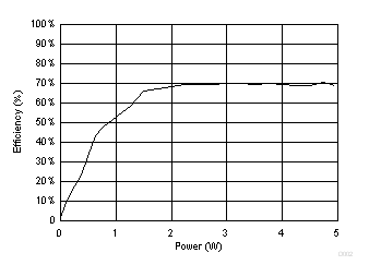
 Figure 11. Efficiency vs Power bq51013B
