SLUSCD3A August 2015 – October 2015
PRODUCTION DATA.
- 1 Features
- 2 Applications
- 3 Description
- 4 Revision History
- 5 Pin Configuration and Functions
- 6 Specifications
-
7 Detailed Description
- 7.1 Overview
- 7.2 Functional Block Diagram
- 7.3
Feature Description
- 7.3.1 A11 Coil Specification
- 7.3.2 Option Select Pins
- 7.3.3 LED Modes
- 7.3.4 Foreign Object Detection (FOD) and FOD Calibration
- 7.3.5 Shut Down Through External Thermal Sensor or Trigger
- 7.3.6 Fault Handling and Indication
- 7.3.7 Power Transfer Start Signal
- 7.3.8 Power-On Reset
- 7.3.9 Trickle Charge and CS100
- 7.4 Device Functional Modes
- 8 Application and Implementation
- 9 Power Supply Recommendations
- 10Layout
- 11Device and Documentation Support
- 12Mechanical, Packaging, and Orderable Information
Package Options
Mechanical Data (Package|Pins)
- RHA|40
Thermal pad, mechanical data (Package|Pins)
- RHA|40
Orderable Information
7 Detailed Description
7.1 Overview
The principle of wireless power transfer is simply an open-cored transformer consisting of transmitter and receiver coils. The transmitter coil and electronics are typically built into a charger pad and the receiver coil and electronics are typically built into a portable device, such as a cell phone. When the receiver coil is positioned on the transmitter coil, magnetic coupling occurs when the transmitter coil is driven. The flux is coupled into the secondary coil, which induces a voltage and current flows. The secondary voltage is rectified, and power can be transferred effectively to a load, wirelessly. Power transfer can be managed through various closed loop control schemes.
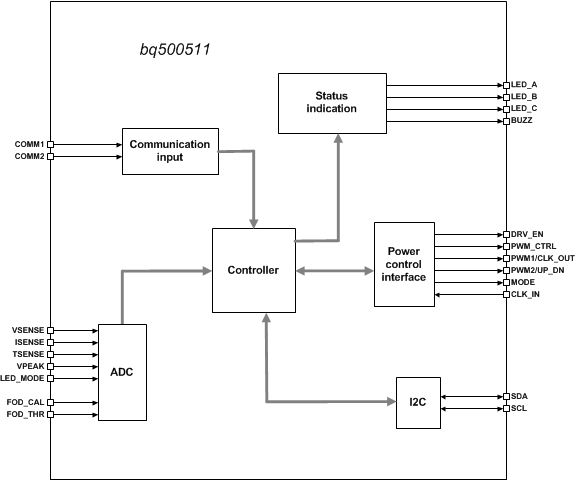
After power is applied and the transmitter device comes out of reset, it will automatically begin the process of detecting and powering a receiver. The bq500511 sends a ping to detect the presence of a receiver on the pad. After a receiver is detected, the bq500511 attempts to establish communication and begin power transfer. The bq500511 is designed to operate with the bq50002 Wireless Power Transmitter Analog Front End to control a full-bridge power stage to drive the primary coil. Through a simple interface the bq500511 instructs the bq50002 how much to increase or decrease power. The full bridge power stage allows for higher power delivery for a given supply voltage.
7.2 Functional Block Diagram
7.3 Feature Description
7.3.1 A11 Coil Specification
The bq500511 controller supports the A11 transmitter coil type for which the coil and matching capacitor specification has been established by the WPC Standard although the device can be used in a proprietary (non-WPC) system. This is fixed and cannot be changed on the transmitter side.
For a current list of coil vendors, see bqTESLA Transmitter Coil Vendors, SLUA649.
7.3.2 Option Select Pins
There are three option select pins on the bq500511. Two (FOD_CAL and FOD_THR) are used to calibrate the foreign object detection algorithm. The third (LED_MODE) selects the LED output behavior. The voltages on these pins will be read by bq500511 at power-up.
For LED_MODE, the selected bin determines the LED behavior based on Table 1.
See section Foreign Object Detection (FOD) and FOD Calibration for more information on the remaining option select pins.
7.3.3 LED Modes
The bq500511 can directly drive three LED outputs (pin 11, pin 12, and pin 14) through a simple current limit resistor (typically 470 Ω), based on the mode selected. The three current limit resistors can be individually adjusted to tune or match the brightness of the LEDs. Do not exceed the maximum output current rating of the device.
Several predefined LED display schemes are selectable via the voltage on the LED_MODE pin at startup. Any means of setting the LED_MODE voltage can be used; if a resistor divider between 3 V and ground is used as shown in Figure 3, relatively large values should be used to minimize the idle power loss. With 100 kΩ used for the upper resistor values for the lower resister, RLED selects one of the desired LED indication schemes presented in Table 1.
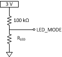 Figure 3. LED_MODE Selection
Table 1. LED Control
| LED CONTROL OPTION |
RLED
SELECTION RESISTOR (kΩ) |
DESCRIPTION | LED | OPERATIONAL STATES | |||||
|---|---|---|---|---|---|---|---|---|---|
| STANDBY | POWER TRANSFER(1) | CHARGE COMPLETE | FAULT(1)(2) | FOD WARNING(2) |
DPL(1) | ||||
| 1 | 24.9 | 2-LED option #1 | LED_A (green) | off | blink slow | on | off | off | blink slow |
| LED_B (red) | off | off | off | on | blink fast | blink slow | |||
| LED_C (orange) | – | – | – | – | – | – | |||
| 2 | 36.5 | 2-LED option Standby LED’s |
LED_A (green) | on | blink slow | on | off | off | blink slow |
| LED_B (red) | on | off | off | on | blink fast | blink slow | |||
| LED_C (orange) | – | – | – | – | – | – | |||
| 3 | 49.9 | Single LED option | LED_A (green) | off | on | off | blink fast | on | on |
| LED_B (red) | – | – | – | – | – | – | |||
| LED_C (orange) | – | – | – | – | – | – | |||
| 4 | 66.5 | 2-LED option #2 | LED_A (green) | off | on | off | off | off | – |
| LED_B (red) | off | off | off | on | blink fast | blink slow | |||
| LED_C (orange) | – | – | – | – | – | – | |||
| 5 | 86.6 | 3-LED option #1 | LED_A (green) | off | off | on | off | off | |
| LED_B (red) | off | on | off | on | on | on | |||
| LED_C (orange) | off | off | off | off | off | off | |||
| 6 | 113 | 3-LED option #2 | LED_A (green) | off | blink slow | on | off | off | off |
| LED_B (red) | off | off | off | on | blink fast | off | |||
| LED_C (orange) | off | off | off | off | off | blink slow | |||
| 7 | 147 | 3-LED option #3 | LED_A (green) | off | blink slow | off | off | off | off |
| LED_B (red) | off | off | on | off | off | off | |||
| LED_C (orange) | off | off | off | on | blink fast | blink slow | |||
| 8 | 200 | 2-LED option #3 | LED_A (green) | off | off | on | blink slow | off | off |
| LED_B (red) | off | on | off | blink slow | on | on | |||
| LED_C (orange) | – | – | – | – | – | – | |||
| 9 | 274 | 2-LED option #4 | LED_A (green) | off | blink slow | on | off | off | blink slow |
| LED_B (red) | off | off | off | on | blink fast | blink slow | |||
| LED_C (orange) | – | – | – | – | – | – | |||
| 10 | 392 | 2-LED option #5 | LED_A (green) | off | on | off | blink fast | on | blink slow |
| LED_B (red) | off | off | on | off | off | off | |||
| LED_C (orange) | – | – | – | – | – | – | |||
7.3.4 Foreign Object Detection (FOD) and FOD Calibration
The bq500511 supports FOD in order to meet the requirements of the WPC v1.2 specification and to protect against the heating of metal objects between coils. Continuously monitoring input power, known losses, and the value of power reported by the receiver device being charged, the bq500511 can estimate how much power is unaccounted for and presumed lost due to metal objects placed in the wireless power transfer path. If this unexpected loss exceeds the threshold set by the FOD resistors, a fault is indicated and power transfer is halted
As the default, the FOD resistors should set a threshold of 400 mW which has been empirically determined using standard WPC FOD test objects (disc, ring and foil). Some tuning might be required as every system will be slightly different. This tuning is best done by trial and error: increase or decrease the loss threshold and retry the system with the standard test objects. The ultimate goal of the FOD feature is safety; to protect misplaced metal objects from becoming hot. Reducing the loss threshold and making the system too sensitive may lead to a false object detection and a bad user experience. Find the balance which best suits the application.
If the application requires disabling FOD, it is possible by tying the FOD_THR pin to 3 V.
NOTE
Disabling FOD results in a TX solution that is not WPC v1.2 compliant.
The FOD_CAL input, can be used to compensate for any load-dependent effect on the power loss. Using a calibrated FOD reference receiver with no foreign objects present, FOD_CAL should be selected such that the calculated loss across the load range is substantially constant (within approximately 100 mW). After correcting for the load dependence, the FOD thresholds should be re-set above the resulting average by approximately 400 mW for the transmitter to satisfy the WPC requirements on tolerated heating.
Similarly to the LED_MODE selection, FOD_THR and FOD_CAL are set based on the voltage of their inputs (pins 35 and 10 respectively) measured when the device is powered up.
Where:
FOD_threshold is the maximum allowed loss in mW, above which a FOD fault is triggered.
FOD_THR is the voltage on pin 35 in volts (between 0 and 2.5 Volts).
For example, to set the recommended starting threshold of 400 mW, 1 V should be applied to FOD_THR; this could be accomplished with a resistor divider between 3 V and ground consisting of 200 kΩ over 100 kΩ.
The value for FOD_CAL is calculated with an offset to allow a correction which either increases or decreases with load.
Where:
FOD_correction is load dependent correction in mW/Amp.
FOD_CAL is the voltage on pin 10 in volts (between 0 and 2.5 Volts).
For both the FOD_THR and FOD_CAL inputs, an internal analog to digital converter with a range of 0 V – 2.5 V is used to measure the input. The combined range and gain provide attainable ranges of 0 mW to 1000 mW for FOD_threshold, and –1000 mW/A to +1000 mW/A for FOD_correction.
Contact TI for the TX tuning tool to set appropriate FOD_THR and FOD_CAL values for your design.
7.3.5 Shut Down Through External Thermal Sensor or Trigger
Typical applications of the bq500511 do not require additional thermal protection. This shutdown feature is provided for enhanced applications and is not limited to thermal shutdown. The key parameter is the 1 V threshold on pin 13, TSENSE. Voltage below 1 V on pin 13 causes the device to shut down. The application of thermal monitoring through a negative temperature coefficient (NTC) sensor, for example, is straightforward. The NTC forms the lower leg of a temperature-dependent voltage divider. The NTC leads are connected to the bq500511 device, pin 13 and GND. The threshold on pin 13 is set to 1 V, below which the system shuts down and indicates a fault (indication depending on LED mode chosen).
To implement this feature follow these steps:
- Consult the NTC data sheet and find the resistance versus temperature curve.
- Determine the actual temperature where the NTC will be placed by using a thermal probe.
- Read the NTC resistance at that temperature in the NTC datasheet, that is R_NTC.
- Use the following formula to determine the upper leg resistor (R_Setpoint):
The system restores normal operation after approximately five minutes or if the receiver is removed. If the feature is not used, this pin must be pulled high.
NOTE
Pin 13, TSENSE, must always be terminated; otherwise, erratic behavior may occur.
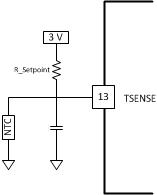 Figure 4. NTC Application (optional)
7.3.6 Fault Handling and Indication
Table 2 shows end power transfer (EPT) packet responses, fault conditions, and the duration of how long the condition lasts until a retry in attempted. The LED mode selected determines how the LED indicates the condition or fault.
Table 2. Fault Handling and Indication
| CONDITION | DURATION(1)
(before retry) |
COMMENTS IMMEDIATE(2) |
|---|---|---|
| EPT-00 | unknown | |
| EPT-01 | 5 seconds | charge complete |
| EPT-02 | Infinite | internal fault |
| EPT-03 | 5 minutes | over temperature |
| EPT-04 | Immediate | over voltage |
| EPT-05 | Immediate | over current |
| EPT-06 | Infinite | battery failure |
| EPT-07 | Not applicable | reconfigure |
| EPT-08 | Immediate | no response |
| OVP | Immediate | TX over voltage |
| NTC | 5 minutes | TX over temperature |
| FOD warning | 12 seconds | buzzer and LED |
| FOD trip | 5 minutes | same as over temp |
7.3.7 Power Transfer Start Signal
The bq500511 provides an output signal to indicate that power transfer has begun. Pin 15, BUZZ, outputs a 400-ms duration, 4-kHz square wave appropriate to drive a low cost AC type ceramic buzzers. If not used, this pin should be left open.
7.3.8 Power-On Reset
The bq500511 has an integrated power-on reset (POR) circuit which monitors the supply voltage and handles the correct device startup sequence. Additional supply voltage supervisor or reset circuits are not needed.
7.3.9 Trickle Charge and CS100
The WPC specification provides an EPT message (EPT–01) to indicate charge complete. Upon receipt of the charge complete message, the bq500511 disables the output and changes the LED indication. The exact indication depends on the LED_MODE chosen. In some battery charging applications, there is a benefit to continue the charging process in trickle-charge mode to top off the battery. The WPC specification provides for an informational 'Charge Status' packet that conveys the level of battery charger. The bq500511 uses this command to enable top-off charging. The bq500511 changes the LED indication to reflect charge complete when a Charge Status message indicating 100% is received, but unlike the response to an EPT, it will not halt power transfer even though the LED indicates charge complete. The mobile device can use a CS100 packet to enable trickle charge mode. If the reported charge status drops below 90%, normal charging indication is resumed.
7.4 Device Functional Modes
7.4.1 Power Transfer
Power transfer efficiency and robustness depends on coil coupling. Coupling depends on the distance between coils, alignment, coil dimensions, coil materials, number of turns, magnetic shielding, impedance matching, frequency, and duty cycle. Most importantly, the receiver and transmitter coils must be aligned for best coupling and efficient power transfer. The smaller the space between the coils is, the better the coupling. Shielding is added as a backing to both the transmitter and receiver coils to direct the magnetic field to the coupled zone. Magnetic fields outside the coupled zone do not transfer power. Thus, shielding also serves to contain the fields to avoid coupling to other adjacent system components.
Regulation can be achieved by controlling any one of the coil coupling parameters. However, for WPC compatibility, the transmitter-side coils and capacitance are specified and the resonant frequency point is fixed. Power transfer is regulated by changing the operating frequency between 110 kHz to 205 kHz. The higher the frequency, the further from resonance and the lower the power. Duty cycle remains constant at 50% throughout the power band and is reduced only once 205 kHz is reached.
7.4.1.1 Dynamic Power Limiting™
Dynamic Power Limiting™ (DPL) allows operation from a 5-V supply with limited current capability (such as a USB port). When the input voltage is observed drooping, the output power is dynamically limited to reduce the load and provides margin relative to the supply’s capability.
Anytime the DPL control loop is regulating the operating point of the transmitter, the LED will indicate that DPL is active. The LED color and flashing pattern are determined by the LED Table. If the receiver sends a Control Error Packet (CEP) with a negative value, (for example, to reduce power to the load), the bq500511 in DPL mode will return to normal operation and respond to this CEP via the standard WPC control loop behavior.
7.4.1.2 Operating Frequency Limiting
Pin-33, FLIM, can be used to set an upper operating frequency limit of 190 kHz by pulling down with a 10-kΩ resistor. Regulatory bodies in some countries have proposed that wireless power transmitters limit operation at this point. While not required anywhere today, this forward looking option provides the means for a simple design modification to address that possible future requirement. A weak internal pull-up allows normal operation without any applied bias.
Note that this feature may prevent WPC certification.
7.4.2 Communication
Communication within the WPC v1.2 specification is from the receiver to the transmitter. For example, in order to regulate the output of the transmitter, the receiver sends messages requesting the transmitter to increase or decrease power. The receiver communicates by modulating the rectifier voltage and using amplitude modulation (AM) sends packets of information to the transmitter. A packet is comprised of a preamble, a header, the actual message, and a checksum, as defined by the WPC standard.
The receiver sends a packet by modulating an impedance network. This AM signal reflects back as a change in the voltage amplitude on the transmitter coil. In the bq500511/bq50002 system, the bq50002 performs the demodulation function and passes a digitized version of the message to the bq500511 where the message is decoded and processed. For example in response to a Control Error Packet, the bq500511 calculates the required change in output power and in turn controls the bq50002 through the CLK_OUT, UP_DOWN, and MODE pins to adjust the operating point and thus its output power.
The modulation impedance network on the receiver can either be resistive or capacitive. Figure 5 shows the resistive modulation approach, where a resistor is periodically added to the load, resulting in an amplitude change in the transmitter voltage. Figure 6 shows the corresponding capacitive modulation approach.
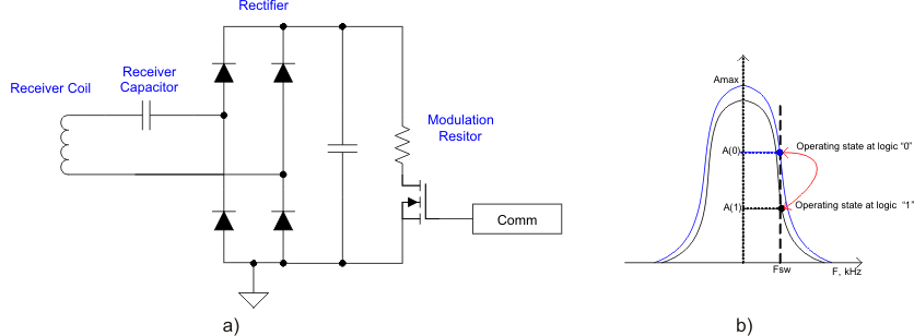 Figure 5. Receiver Resistive Modulation Circuit
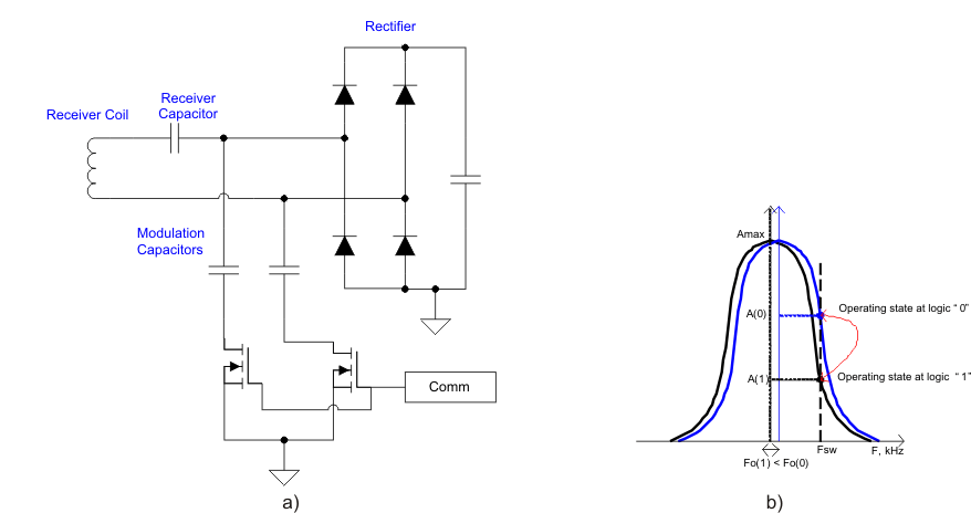 Figure 6. Receiver Capacitive Modulation Circuit