SLUSBS9A February 2014 – July 2014
PRODUCTION DATA.
- 1 Features
- 2 Applications
- 3 Description
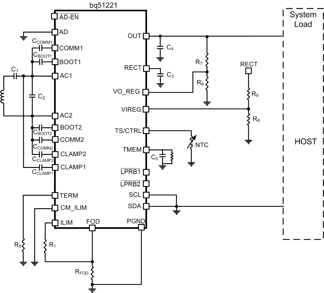
- 4 Simplified Schematic
- 5 Revision History
- 6 Device Comparison Table
- 7 Pin Configuration and Functions
- 8 Specifications
-
9 Detailed Description
- 9.1 Overview
- 9.2 Functional Block Diagram
- 9.3
Feature Description
- 9.3.1 Dynamic Rectifier Control
- 9.3.2 Dynamic Power Scaling
- 9.3.3 VO_REG and VIREG Calculations
- 9.3.4 RILIM Calculations
- 9.3.5 Adapter Enable Functionality
- 9.3.6 Turning Off the Transmitter
- 9.3.7 CM_ILIM
- 9.3.8 PD_DET and TMEM
- 9.3.9 TS, Both WPC and PMA
- 9.3.10 I2C Communication
- 9.3.11 Input Overvoltage
- 9.4 Device Functional Modes
- 9.5 Register Maps
-
10Application and Implementation
- 10.1 Application Information
- 10.2
Typical Applications
- 10.2.1
Dual Mode Design (WPC and PMA Compliant) Power Supply 5-V Output With 1-A Maximum Current
- 10.2.1.1 Design Requirements
- 10.2.1.2
Detailed Design Procedure
- 10.2.1.2.1 Output Voltage Set Point
- 10.2.1.2.2 Output and Rectifier Capacitors
- 10.2.1.2.3 Maximum Output Current Set Point
- 10.2.1.2.4 TERM Resistor
- 10.2.1.2.5 Setting LPRB1 and LPRB2 Resistors
- 10.2.1.2.6 I2C
- 10.2.1.2.7 Communication Current Limit
- 10.2.1.2.8 Receiver Coil
- 10.2.1.2.9 Series and Parallel Resonant Capacitors
- 10.2.1.2.10 Communication, Boot and Clamp Capacitors
- 10.2.1.3 Application Curves
- 10.2.2 bq51221 Embedded in System Board
- 10.2.3 bq51221 Implemented in Back Cover
- 10.2.1
Dual Mode Design (WPC and PMA Compliant) Power Supply 5-V Output With 1-A Maximum Current
- 11Power Supply Recommendations
- 12Layout
- 13Device and Documentation Support
- 14Mechanical, Packaging, and Orderable Information
Package Options
Mechanical Data (Package|Pins)
- YFP|42
Thermal pad, mechanical data (Package|Pins)
Orderable Information
1 Features
- Robust 5-W Solution With 50% Lower Losses for Improved Thermals
- Inductorless Receiver for Lowest Height Profile Solution
- Adjustable Output Voltage (4.5 to 8 V) for Coil and Thermal Optimization
- Fully Synchronous Rectifier With 96% Efficiency
- 97% Efficient Post Regulator
- 79% System Efficiency at 5 W
- WPC v1.1 and PMA Compliant Communication
- Patented Transmitter Pad Detect Function Improves User Experience
- I2C Communication with Host
2 Applications
- Smart Phones, Tablets, and Headsets
- Wi-Fi Hotspots
- Power Banks
- Other Handheld Devices
3 Description
The bq51221 device is a fully contained wireless power receiver capable of operating in both the WPC and PMA protocols which allows a wireless power system to work with both WPC and PMA inductive charging standards. The bq51221 device provides a single device power conversion (rectification and regulation) as well as the digital control and communication for both standards. It also has autonomous detection of protocol and requires no additional active devices. The bq51221 device complies with the WPC v1.1 and PMA communication protocol. Together with the WPC or a PMA primary-side controller, the bq51221 device enables a complete wireless power transfer system for a wireless power supply solution. The receiver allows for synchronous rectification, regulation and control and communication to all exist in a market-leading form factor, efficiency, and solution size.
Device Information(1)
| PART NUMBER | PACKAGE | BODY SIZE (MAX) |
|---|---|---|
| bq51221 | YFP (42) | 3.586 mm × 2.874 mm |
- For all available packages, see the orderable addendum at the end of the data sheet.
4 Simplified Schematic
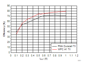
bq51221 Dual Mode Efficiency 5-V Out