SLUSBS9A February 2014 – July 2014
PRODUCTION DATA.
- 1 Features
- 2 Applications
- 3 Description
- 4 Simplified Schematic
- 5 Revision History
- 6 Device Comparison Table
- 7 Pin Configuration and Functions
- 8 Specifications
-
9 Detailed Description
- 9.1 Overview
- 9.2 Functional Block Diagram
- 9.3
Feature Description
- 9.3.1 Dynamic Rectifier Control
- 9.3.2 Dynamic Power Scaling
- 9.3.3 VO_REG and VIREG Calculations
- 9.3.4 RILIM Calculations
- 9.3.5 Adapter Enable Functionality
- 9.3.6 Turning Off the Transmitter
- 9.3.7 CM_ILIM
- 9.3.8 PD_DET and TMEM
- 9.3.9 TS, Both WPC and PMA
- 9.3.10 I2C Communication
- 9.3.11 Input Overvoltage
- 9.4 Device Functional Modes
- 9.5 Register Maps
-
10Application and Implementation
- 10.1 Application Information
- 10.2
Typical Applications
- 10.2.1
Dual Mode Design (WPC and PMA Compliant) Power Supply 5-V Output With 1-A Maximum Current
- 10.2.1.1 Design Requirements
- 10.2.1.2
Detailed Design Procedure
- 10.2.1.2.1 Output Voltage Set Point
- 10.2.1.2.2 Output and Rectifier Capacitors
- 10.2.1.2.3 Maximum Output Current Set Point
- 10.2.1.2.4 TERM Resistor
- 10.2.1.2.5 Setting LPRB1 and LPRB2 Resistors
- 10.2.1.2.6 I2C
- 10.2.1.2.7 Communication Current Limit
- 10.2.1.2.8 Receiver Coil
- 10.2.1.2.9 Series and Parallel Resonant Capacitors
- 10.2.1.2.10 Communication, Boot and Clamp Capacitors
- 10.2.1.3 Application Curves
- 10.2.2 bq51221 Embedded in System Board
- 10.2.3 bq51221 Implemented in Back Cover
- 10.2.1
Dual Mode Design (WPC and PMA Compliant) Power Supply 5-V Output With 1-A Maximum Current
- 11Power Supply Recommendations
- 12Layout
- 13Device and Documentation Support
- 14Mechanical, Packaging, and Orderable Information
Package Options
Mechanical Data (Package|Pins)
- YFP|42
Thermal pad, mechanical data (Package|Pins)
Orderable Information
9 Detailed Description
9.1 Overview
Both WPC and PMA wireless power systems consist of a charging pad (primary, transmitter) and the secondary-side equipment (receiver). There are coils in the charging pad and secondary equipment, which magnetically couple to each other when the receiver is placed on the transmitter. Power is transferred from the primary to the secondary by transformer action between the coils. The receiver can achieve control over the amount of power transferred by getting the transmitter to change the field strength by changing the frequency, or duty cycle, or voltage rail energizing the primary coil.
The receiver equipment communicates with the primary by modulating the load seen by the primary. This load modulation results in a change in the primary coil current or primary coil voltage, or both, which is measured and demodulated by the transmitter.
In WPC, the system communication is digital — packets that are transferred from the secondary to the primary. Differential bi-phase encoding is used for the packets. The bit rate is 2 kb/s. Various types of communication packets are defined. These include identification and authentication packets, error packets, control packets, power usage packets, and end power transfer packets, among others.
A PMA-compliant receiver communicates based on continuous transmission of signals from the receiver to the transmitter. The PMA specification defines six different communications symbols. These are increment (INC), decrement (DEC), no change (NoCh), end of charge (EOC), MsgBit, and a symbol for future use. Each PMA receiver has a unique PMA RXID, which is a 6-byte unique message that is sent to the PMA TX at startup.
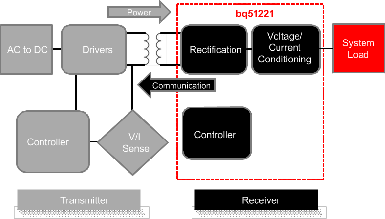 Figure 7. Dual Mode Wireless Power System Indicating the Functional Integration of the bq51221 Family
The bq51221 device integrates fully-compliant WPC v1.1 and PMA communication protocols in order to streamline the dual mode receiver designs (no extra software development required). Other unique algorithms such as Dynamic Rectifier Control are integrated to provide best-in-class system efficiency while keeping the smallest solution size of the industry.
As a WPC system, when the receiver shown in Figure 7 is placed on the charging pad, the secondary coil couples to the magnetic flux generated by the coil in the transmitter, which consequently induces a voltage in the secondary coil. The internal synchronous rectifier feeds this voltage to the RECT pin, which in turn feeds the LDO which feeds the output.
The bq51221 device identifies and authenticates itself to the primary using the COMMx pins, switching on and off the COMM FETs, and hence switching in and out COMM capacitors. If the authentication is successful, the primary remains powered-up. The bq51221 device measures the voltage at the RECT pin, calculates the difference between the actual voltage and the desired voltage VRECT(REG), and sends back error packets to the transmitter. This process goes on until the input voltage settles at VRECT(REG) MAX. During a load change, the dynamic rectifier algorithm sets the targets specified by targets between VRECT(REG) MAX and VRECT(REG) MIN shown in Table 1 . This algorithm enhances the transient response of the power supply.
After the voltage at the RECT pin is at the desired value, a pass FET is enabled. The voltage control loop ensures that the output voltage is maintained at VOUT(REG), powering the downstream charger. The bq51221 device meanwhile continues to monitor the input voltage, and keeps sending control error packets (CEP) to the primary on average every 250 ms. If a large transient occurs, the feedback to the primary speeds up to 32-ms communication periods to converge on an operating point in less time.
If the receiver shown in Figure 7 is used with a PMA transmitter, the bq51221 device identifies itself to the PMA transmitter using the COMMx pins. If sufficient power is delivered to the bq51221 device to wake up the device, it responds by modulating the power signal according to the PMA communication protocol. Prior to enabling the output, the bq51221 device transmits an RXID message. This is a unique identification message that is controlled through an IEEE sanctioned database and every bq51221 device comes programmed with its own unique RXID that can be read back using I2C. Please see I2C register map in Register Maps for details on the location of the RXID. The bq51221 device then monitors the voltage at the RECT pin. If there is a difference between the actual voltage and the desired voltage VRECT(REG), the device sends a PMA DEC or PMA INC signal to the PMA transmitter to control the RECT voltage to be within the desired window. The receiver regulates VRECT to a desired window of operation shown inFigure 15).
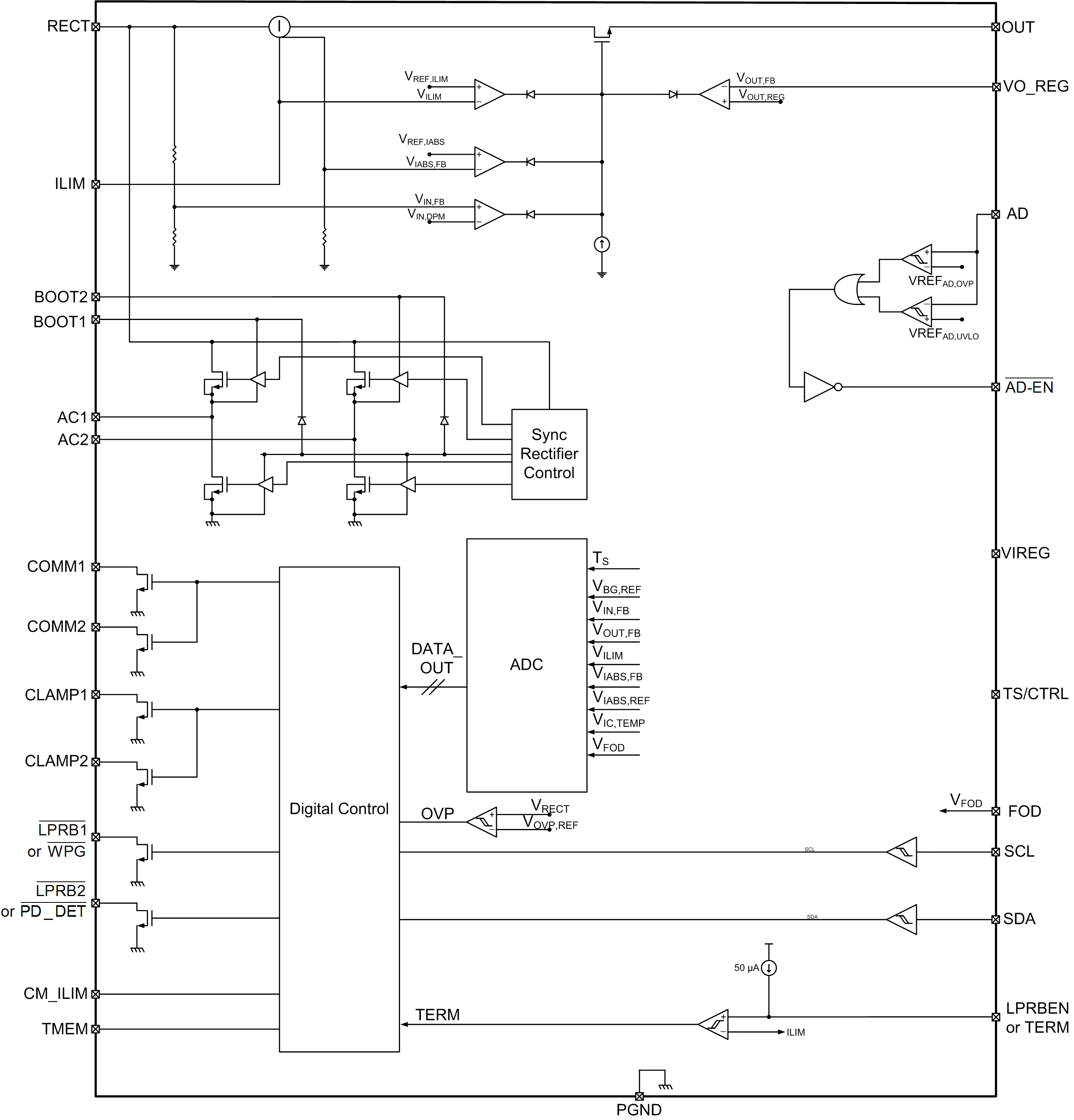
9.2 Functional Block Diagram
9.3 Feature Description
9.3.1 Dynamic Rectifier Control
WPC Mode Only
The Dynamic Rectifier Control algorithm offers the end system designer optimal transient response for a given maximum output current setting. This is achieved by providing enough voltage headroom across the internal regulator (LDO) at light loads in order to maintain regulation during a load transient. The WPC system has a relatively slow global feedback loop where it can take up to 150 ms to converge on a new rectifier voltage target. Therefore, a transient response is dependent on the loosely coupled transformer's output impedance profile. The Dynamic Rectifier Control allows for a 1.5-V change in rectified voltage before the transient response is observed at the output of the internal regulator (output of the bq51221 device). A 1-A application allows up to a 2-Ω output impedance. The Dynamic Rectifier Control behavior is illustrated in Figure 13 where RILIM is set to 680 Ω.
9.3.2 Dynamic Power Scaling
WPC Mode Only
The Dynamic Power Scaling feature allows for the loss characteristics of the bq51221 device to be scaled based on the maximum expected output power in the end application. This effectively optimizes the efficiency for each application. This feature is achieved by scaling the loss of the internal LDO based on a percentage of the maximum output current. Note that the maximum output current is set by the KILIM term and the RILIM resistance (where RILIM = KILIM / IILIM). The flow diagram in Figure 13 shows how the rectifier is dynamically controlled (Dynamic Rectifier Control) based on a fixed percentage of the IILIM setting. Table 1 summarizes how the rectifier behavior is dynamically adjusted based on two different RILIM settings. The table is shown for IMAX, which is typically lower than IILIM (about 20% lower). See RILIM Calculations for more details.
Table 1. Dynamic Rectifier Regulation
| Output Current Percentage | RILIM = 1400 Ω IMAX = 0.5 A |
RILIM = 700 Ω IMAX = 1.0 A |
VRECT |
|---|---|---|---|
| 0 to 10% | 0 to 0.05 A | 0 to 0.1 A | VOUT + 2 |
| 10 to 20% | 0.05 to 0.1 A | 0.1 to 0.2 A | VOUT + 1.68 |
| 20 to 40% | 0.1 to 0.2 A | 0.2 to 0.4 A | VOUT + 0.56 |
| >40% | >0.2 A | >0.4 A | VOUT + 0.12 |
Dynamic Rectifier Control shows the shift in the dynamic rectifier control behavior based on the two different RILIM settings. With the rectifier voltage (VRECT) being the input to the internal LDO, this adjustment in the Dynamic Rectifier Control thresholds dynamically adjusts the power dissipation across the LDO where,

Figure 26 shows how the system efficiency is improved due to the Dynamic Power Scaling feature. Note that this feature balances efficiency with optimal system transient response.
9.3.3 VO_REG and VIREG Calculations
WPC and PMA Modes
The bq51221 device allows the designer to set the output voltage by setting a feedback resistor divider network from the OUT pin to the VO_REG pin as seen in Figure 8. The resistor divider network should be chosen so that the voltage at the VO_REG pin is 0.5 V at the desired output voltage. This applies to the default I2C code for VO_REG shown in I2C register 0x01 shown in Table 5 (Bits B0, B1, B2).
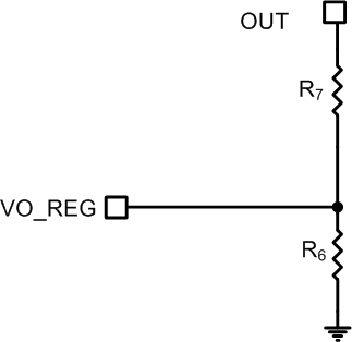 Figure 8. VO_REG Network
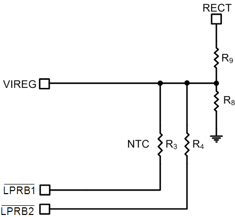 Figure 9. VIREG Network (For PMA)
Choose the desired output voltage VOUT and R6:


After R6 and R7 are chosen, the same divider network is attached to VIREG pin from RECT to GND, as shown in Figure 9. R9 = R7 and R8 = R6
LPRB1 and LPRB2 are two additional pins that are used to implement a back cover solution and are used for PMA (see Figure 41). In a back cover solution where the system designer cannot depend on the characteristics of the downstream charger in the phone, these pins can be used to boost the rectifier at a lower power (Low Power Rectifier Boost), so that the system is able to survive a load transient from 0 mA to the maximum current by boosting the rectifier during low power output that the system is designed for. See resistor calculations for LPRB1 and LPRB2: in the bq51221 web page "Tools & software" tab. The Excel file not only provides how to calculate the LPRB resistor values but also assists with other calculations. The Excel file can be accessed at www.ti.com/product/bq51221/toolssoftware.
Table 2. LPRB Condition Table
| IOUT | LPRB1 | LPRB2 |
|---|---|---|
| 0 mA < IOUT < 100 mA | ON | ON |
| 100 mA < IOUT < 350 mA | OFF | ON |
| 350 mA < IOUT < Maximum current | OFF | OFF |
The LPRB1 and LPRB2 resistors can be omitted in an embedded solution where the system designer is in control of the voltage at which the downstream charger can regulate the input current to prevent the input from collapsing in a load transient (VIN-DPM). The functionality of LPRB1 and LPRB2 can be reverted to WPG and PD_DET by not populating the TERM resistor. In this case, the host enables the charge complete on the TS/CTRL pin by pulling this pin high.
For the back cover solution, the TERM resistor is populated and this enables LPRB1 and LPRB2 functionality. The functionality can be seen in Table 2.
9.3.4 RILIM Calculations
WPC and PMA Modes
The bq51221 device includes a means of providing hardware overcurrent protection (IILIM) through an analog current regulation loop. The hardware current limit provides an extra level of safety by clamping the maximum allowable output current (for example, current compliance). The RILIM resistor size also sets the thresholds for the dynamic rectifier levels providing efficiency tuning per each application’s maximum system current. The calculation for the total RILIM resistance is as follows:
RILIM allows for the ILIM pin to reach 1.2 V at an output current equal to IILIM. When choosing RILIM, two options are possible.
If the user's application requires an output current equal to or greater than the external IILIM that the circuit is designed for (input current limit on the charger where the receiver device is tied higher than the external IILIM), ensure that the downstream charger is capable of regulating the voltage of the input into which the receiver device output is tied to by lowering the amount of current being drawn. This ensures that the receiver output does not drop to 0 V. Such behavior is referred to as Dynamic Power Management (VIN-DPM) in TI chargers. Unless such behavior is enabled on the charger, the charger will pull the output of the receiver device to ground when the receiver device enters current regulation. If the user's applications are designed to extract less than the IILIM (1-A maximum), typical designs should leave a design margin of at least 10%, so that the voltage at ILIM pin reaches 1.2 V when 10% more than maximum current is drawn from the output. Such a design would have input current limit on the charger lower than the external ILIM of the receiver device. In both cases however, the charger must be capable of regulating the current drawn from the device to allow the output voltage to stay at a reasonable value. This same behavior is also necessary during the WPC communication. The following calculations show how such a design is achieved:
where
When referring to the application diagram shown in Typical Applications, RILIM is the sum of the R1 and RFOD resistance (that is, the total resistance from the ILIM pin to GND). RFOD is chosen according to the application. The tool for calculating RFOD can be obtained by contacting your TI representative. Use RFOD to allow the receiver implementation to comply with WPC v1.1 requirements related to received power accuracy.
9.3.5 Adapter Enable Functionality
WPC and PMA Modes
The bq51221 device can also help manage the multiplexing of adapter power to the output and can shut off the TX when the adapter is plugged in and is above the VAD-EN. After the adapter is plugged in and the output turns off, the RX device sends an EOC to the TX. In this case, the AD_EN pins are then pulled to approximately 4 V below AD, which allows the device turn on the back-to-back PMOS connected between AD and OUT (Figure 40).
Both the AD and AD-EN pins are rated at 30 V, while the OUT pin is rated at 20 V. It must also be noted that it is required to connect a back-to-back PMOS between AD and OUT so that voltage is blocked in both directions. Also, when AD mode is enabled, no load can be pulled from the RECT pin as this could cause an internal device overvoltage in the bq51221 device.
9.3.6 Turning Off the Transmitter
WPC and PMA Modes
Both specifications allow the receiver to turn off the transmitter and put the system in a low-power standby mode. There are two different ways to accomplish this with the bq51221 device. In both modes, the EPT charge complete (WPC) or end of charge (PMA) can be sent to the TX by pulling the TS pin high (above 1.4 V). The bq51221 device will then sense this and send the appropriate signal to the TX, thus putting the TX in a low power standby mode.
9.3.6.1 WPC End Power Transfer (EPT)
The WPC allows for a special command to terminate power transfer from the TX termed EPT packet. The v1.1 specifies the following reasons and their responding data field value in Table 3.
Table 3. End Power Transfer Codes in WPC
| Reason | Value | Condition(1) |
|---|---|---|
| Unknown | 0x00 | AD > 3.6 V |
| Charge Complete | 0x01 | TS/CTRL = 1 |
| Internal Fault | 0x02 | TJ > 150°C or RILIM < 215 Ω |
| Over Temperature | 0x03 | TS < VTS-HOT, or TS/CTRL < 100 mV(3) |
| Over Voltage | 0x04 | VRECT target does not converge(2) |
| Over Current | 0x05 | Not sent |
| Battery Failure | 0x06 | Not sent |
| Reconfigure | 0x07 | Not sent |
| No Response | 0x08 | Not sent |
9.3.6.2 PMA EOC
PMA EOC is a state where the bq51221 device disables the output and sends EOC frequency to terminate the power transfer on a PMA transmitter. This can be done by setting the TERM pin resistor so that the voltage on the TERM pin is higher than the ILIM pin at the desired termination current. This TERM resistor method of sending the EOC to the transmitter only works with PMA TX. After the TERM resistor is populated, it also changes the behavior of the LPRBx pins. Check the section on LPRBx resistors for more information. Another way to send an EOC to the PMA TX is to pull the TS pin above 1.4 V through an external pullup.
9.3.7 CM_ILIM
WPC Mode Only
Communication current limit is a feature that allows for error free communication to happen between the RX and TX in the WPC mode. This is done by decoupling the coil from the load transients by limiting the output current during communication with the TX. The communication current limit is set according to Table 4. The communication current limit can be disabled by pulling CM_ILIM pin high (> 1.4 V) or enabled by pulling the CM_ILIM pin low. There is an internal pulldown that enables communication current limit when the CM_ILIM pin is left floating.
Table 4. Communication Current Limit Table
| IOUT | Communication Current Limit |
|---|---|
| 0 mA < IOUT < 100 mA | None |
| 100 mA < IOUT < 400 mA | IOUT + 50 mA |
| 400 mA < IOUT < Max current | IOUT – 50 mA |
When the communication current limit is enabled, the amount of current that the load can draw is limited. If the charger in the system does not have a VIN-DPM feature, the output of the receiver will collapse if communication current limit is enabled. In order to disable Communication Current Limit, pull CM_ILIM pin high.
9.3.8 PD_DET and TMEM
PD_DET is only available in WPC mode. This is an open-drain pin that goes low based on the voltage of the TMEM pin. When the voltage of TMEM is higher than 1.6 V, PD_DET will be low. The voltage on the TMEM pin depends on capturing the energy from the digital ping from the transmitter and storing it on the C5 capacitor in Figure 10. After the receiver sends an EPT (charge complete), the transmitter shuts down and goes into a low-power mode. However, it will continue to check if the receiver would like to renegotiate a power transfer by periodically performing the digital ping. The energy from the digital ping can be stored on the TMEM pin until the next digital ping refreshes the capacitor. A bleedoff resistor RMEMcan be chosen in parallel with C5 that sets the time constant so that the TMEM pin will fall below 1.6 V once the next ping timer expires. The duration between digital pings is indeterminate and depends on each transmitter manufacturer.
 Figure 10. TMEM Configuration
Set capacitor on C5 = TMEM to 2.2 µF. Resistor RMEM across C5 can be set by understanding the duration between digital pings (tping). Set the resistor such that:

9.3.9 TS, Both WPC and PMA
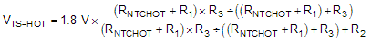
The bq51221 device includes a ratio metric external temperature sense function. The temperature sense function has a low ratio metric threshold which represents a hot condition. TI recommends an external temperature sensor in order to provide safe operating conditions for the receiver product. This pin is best used for monitoring the surface that can be exposed to the end user (for example, place the negative temperature coefficient (NTC) resistor closest to the user touch point on the back cover). A resistor in series or parallel can be inserted to adjust the NTC to match the trip point of the device. The implementation in Figure 11 shows the series-parallel resistor implementation for setting the threshold at which VTS-HOT is reached. Once VTS-HOT is reached, the device will send an EPT – overtemperature signal for a WPC transmitter or an EOC signal to a PMA transmitter depending on the mode the device is operating in. An Excel tool to assist with defining the correct resistor values is available on the bq51221 web folder under 'Tools & Software'. The Excel file can be found at www.ti.com/product/bq51221/toolssoftware.
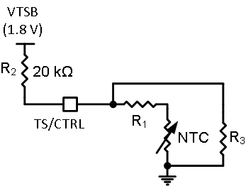 Figure 11. NTC Resistor Setup
Figure 11 shows a parallel resistor setup that can be used to adjust the trip point of VTS-HOT. After the NTC is chosen and RNTCHOT at VTS-HOT is determined from the data sheet of the NTC, Equation 9 can be used to calculate R1 and R3. In many cases depending on the NTC resistor, R1 or R3 can be omitted. When calculating VTS-HOT, omit R1 by setting it to 0 Ω, and omit R3 by setting it to 10 MΩ.
9.3.10 I2C Communication
WPC and PMA Modes
The bq51221 device allows for I2C communication with the internal CPU. In case the I2C is not used, ground SCL and SDA. See Register Maps for more information.
9.3.11 Input Overvoltage
WPC and PMA Modes
If the input voltage suddenly increases in potential for some condition (for example a change in position of the equipment on the charging pad), the voltage-control loop inside the bq51221 device becomes active, and prevents the output from going beyond VOUT(REG). The receiver then starts sending back error packets every 30 ms until the input voltage comes back to an acceptable level, and then maintains the error communication every 250 ms.
If the input voltage increases in potential beyond VRECT-OVP, the device switches off the LDO and informs the primary to bring the voltage back to VRECT(REG). In addition, a proprietary voltage protection circuit is activated by means of CCLAMP1 and CCLAMP2 that protects the device from voltages beyond the maximum rating of the device.
9.4 Device Functional Modes
In WPC mode, at startup operation, the bq51221 device must comply with proper handshaking in order to be granted a power contract from the WPC transmitter. The transmitter initiates the handshake by providing an extended digital ping after analog ping detects an object on the transmitter surface. If a receiver is present on the transmitter surface, the receiver then provides the signal strength, configuration, and identification packets to the transmitter (see volume 1 of the WPC specification for details on each packet). These are the first three packets sent to the transmitter. The only exception is if there is a true shutdown condition on the AD, or TS/CTRL pins where the receiver shuts down the transmitter immediately. See Table 3 for details. After the transmitter has successfully received the signal strength, configuration, and identification packets, the receiver is granted a power contract and is then allowed to control the operating point of the power transfer. With the use of the bq51221 device Dynamic Rectifier Control algorithm, the receiver will inform the transmitter to adjust the rectifier voltage above 8 V prior to enabling the output supply. This method enhances the transient performance during system startup. For the startup flow diagram details, see Figure 12.
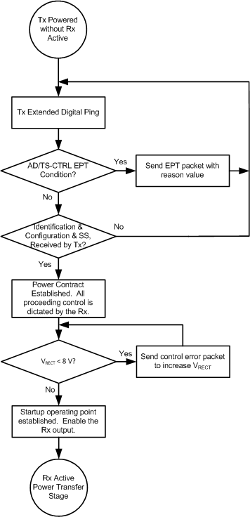 Figure 12. Wireless Power Startup Flow Diagram on WPC TX
After the startup procedure has been established, the receiver will enter the active power transfer stage. This is considered the main loop of operation. The Dynamic Rectifier Control algorithm determines the rectifier voltage target based on a percentage of the maximum output current level setting (set by KILIM and the RILIM). The receiver will send control error packets in order to converge on these targets. As the output current changes, the rectifier voltage target dynamically changes. As a note, the feedback loop of the WPC system is relatively slow, it can take up to 150 ms to converge on a new rectifier voltage target. It should be understood that the instantaneous transient response of the system is open loop and dependent on the receiver coil output impedance at that operating point. The main loop also determines if any conditions in Table 3 are true in order to discontinue power transfer. Figure 13 shows the active power transfer loop.
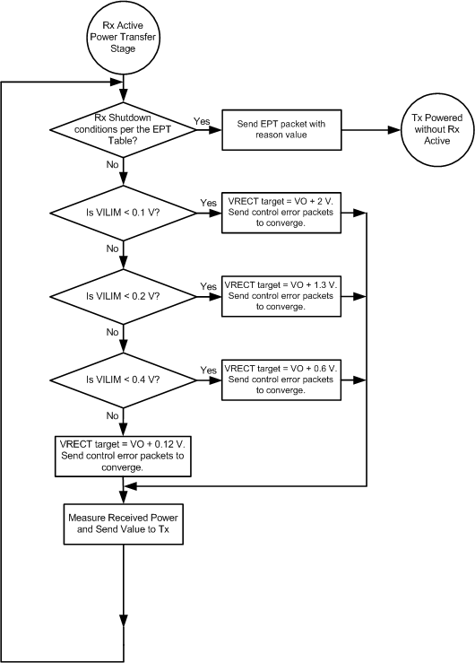 Figure 13. Active Power Transfer Flow Diagram on WPC TX
In PMA mode, during startup operation, PMA transmitter generates a digital ping in a predefined structure regarding the frequencies and timing. If the power delivered during the digital ping is sufficient to wake up the bq51221 device, it responds by modulating the power signal according to the PMA communication protocol. If the transmitter receives a valid PMA signal from the receiver, it continues to the identification phase, without removing the power signal. The receiver continues to send PMA DEC or PMA INC signals until target VRECT is achieved, and after desired VRECT is achieved, the bq51221 device sends a PMA NoCh signal to indicate that no further change is needed in transmitter frequency. Please note unlike the WPC mode receiver, in PMA mode, the bq51221 device will continue to send the PMA NoCh signal if the target VRECT is within a defined voltage range. This means that the device will regulate the VRECT voltage within an acceptable window. This can be seen in Figure 15.
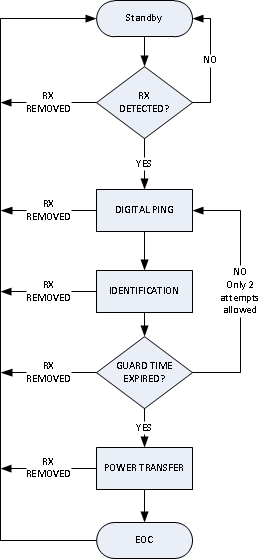 Figure 14. Active Power Transfer Flow Diagram on PMA TX Type 1
Optimized rectification voltage is key to maintaining high efficiency on the bq51221. Figure 15indicates the control and communication protocol between the receiver and the transmitter. The bq51221 sends an increment signal (INC) for increasing the operating frequency of the transmitter to decrease the transferred power if the rectification voltage is above VREFHI_H. INC signals will occur until the rectification voltage is below VREFHI_L. If the rectification voltage is below VREFLO_L then the bq51221 will send a decrease signal (DEC) to the transmitter which will decrease the frequency resulting in increased power delivery. VREFLO_H is the hysteresis level for terminating the DEC signal. A no change signal (NoCh) is sent when the rectification voltage is between VREFLO_H and VREFHI_L indicating there is no need to increase or decrease the transferred power. Additionally, the Hysteresis zones can be NoCh depending on the direction entered. For example, if the rectification voltage moves through VREFHI_L to enter Hysteresis, the NoCh command is sent. If the same Hysteresis zone is entered through VREFHI_H then the INC will continue to be sent until it reaches VREFHI_L where the NoCh signal will commence. The device will not react to a change in load while the rectification voltage falls within the indicated levels (VREFHI_H > VRECT > VREFLO_L). When a load change occurs sufficient to move VRECT outside this range, the appropriate signal (INC or DEC) will be sent.
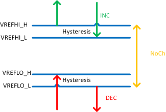 Figure 15. PMA Active Power Control Diagram
9.5 Register Maps
Locations 0x01 and 0x02 can be written to any time. Locations 0xE0 to 0xFF are only functional when VRECT > VUVLO. When VRECT goes below VUVLO, locations 0xE0 to 0xFF are reset.
Table 5. Wireless Power Supply Current Register 1 (READ / WRITE)
| Memory Location: 0x01, Default State: 00000001 | |||
|---|---|---|---|
| BIT | NAME | READ / WRITE | FUNCTION |
| B7 (MSB) | Read / Write | Not used | |
| B6 | Read / Write | Not used | |
| B5 | Read / Write | Not used | |
| B4 | Read / Write | Not used | |
| B3 | Read / Write | Not used | |
| B2 | VOREG2 | Read / Write | 450, 500, 550, 600, 650, 700, 750, or 800 mV Changes VO_REG target Default value 001 |
| B1 | VOREG1 | Read / Write | |
| B0 | VOREG0 | Read / Write | |
Table 6. Wireless Power Supply Current Register 2 (READ / WRITE)
Table 7. I2C Mailbox Register (READ / WRITE)
Table 8. Wireless Power Supply FOD RAM (READ / WRITE)
| Memory Location: 0xE1, Reset State: 00000000(1) | ||||
|---|---|---|---|---|
| BIT | NAME | READ / WRITE | FUNCTION | |
| B7 (MSB) | ESR_ENABLE | Read / Write | Enables I2C based ESR in received power, Enable = 1, Disable = 0 | |
| B6 | OFF_ENABLE | Read / Write | Enables I2C based offset power, Enable = 1, Disable = 0 | |
| B5 | RoFOD5 | Read / Write | 000 – 0 mW 001 -- +39 mW 010 -- +78 mW 011 -- +117 mW 100 -- +156 mW |
101 -- +195 mW 110 -- +234 mW 111 -- +273 mW The value is added to received power message |
| B4 | RoFOD4 | Read / Write | ||
| B3 | RoFOD3 | Read / Write | ||
| B2 | RsFOD2 | Read / Write | 000 – ESR 001 – ESR 010 – ESR × 2 011 – ESR × 3 |
100 – ESR x 4 101 – ESR 110 – ESR 111 – ESR x 0.5 |
| B1 | RsFOD1 | Read / Write | ||
| B0 | RsFOD0 | Read / Write | ||
Table 9. Wireless Power User Header RAM (WRITE)
| Memory Location: 0xE2, Reset State: 00000000(1) | |
|---|---|
| BIT | READ / WRITE |
| B7 (MSB) | Read / Write |
| B6 | Read / Write |
| B5 | Read / Write |
| B4 | Read / Write |
| B3 | Read / Write |
| B2 | Read / Write |
| B1 | Read / Write |
| B0 | Read / Write |
Table 10. Wireless Power USER VRECT Status RAM (READ)
| Memory Location: 0xE3, Reset State: 00000000 Range – 0 to 12 V This register reads back the VRECT voltage with LSB = 46 mV |
|||
|---|---|---|---|
| BIT | NAME | READ / WRITE | FUNCTION |
| B7 (MSB) | VRECT7 | Read | LSB = 46 mV |
| B6 | VRECT6 | Read | |
| B5 | VRECT5 | Read | |
| B4 | VRECT4 | Read | |
| B3 | VRECT3 | Read | |
| B2 | VRECT2 | Read | |
| B1 | VRECT1 | Read | |
| B0 | VRECT0 | Read | |
Table 11. Wireless Power VOUT Status RAM (READ)
| Memory Location: 0xE4, Reset State: 00000000 This register reads back the VOUT voltage with LSB = 46 mV |
|||
|---|---|---|---|
| BIT | NAME | Read / Write | FUNCTION |
| B7 (MSB) | VOUT7 | Read / Write | LSB = 46 mV |
| B6 | VOUT6 | Read / Write | |
| B5 | VOUT5 | Read / Write | |
| B4 | VOUT4 | Read / Write | |
| B3 | VOUT3 | Read / Write | |
| B2 | VOUT2 | Read / Write | |
| B1 | VOUT1 | Read / Write | |
| B0 | VOUT0 | Read / Write | |
Table 12. Wireless Power REC PWR Byte Status RAM (READ)
| Memory Location: 0xE8, Reset State: 00000000 This register reads back the received power with LSB = 39 mW |
|
|---|---|
| BIT | Read / Write |
| B7 (MSB) | Read / Write |
| B6 | Read / Write |
| B5 | Read / Write |
| B4 | Read / Write |
| B3 | Read / Write |
| B2 | Read / Write |
| B1 | Read / Write |
| B0 | Read / Write |
Table 13. Wireless Power Mode Indicator (READ)
| Memory Location: 0xEF, Reset State: 00000000 This register reads back the MODE (WPC or PMA) based on the Transmitter |
|||
|---|---|---|---|
| BIT | NAME | READ / WRITE | FUNCTION |
| B7 (MSB) | Read / Write | Not Used | |
| B6 | ALIGN Status | Read | Alignment mode = 1, Normal operation = 0 (Status bit) |
| B5 | Read / Write | Not Used | |
| B4 | Read / Write | Not Used | |
| B3 | Read / Write | Not Used | |
| B2 | Read / Write | Not Used | |
| B1 | Read / Write | Not Used | |
| B0 | Mode | Read | PMA = 1, WPC = 0 (Status bit) |
Table 14. Wireless Power Prop Packet Payload RAM Byte 0 (WRITE)
| Memory Location: 0xF1, Reset State: 00000000 | |
|---|---|
| BIT | Read / Write |
| B7 (MSB) | Read / Write |
| B6 | Read / Write |
| B5 | Read / Write |
| B4 | Read / Write |
| B3 | Read / Write |
| B2 | Read / Write |
| B1 | Read / Write |
| B0 | Read / Write |
Table 15. Wireless Power Prop Packet Payload RAM Byte 1 (WRITE)
| Memory Location: 0xF2, Reset State: 00000000 | |
|---|---|
| BIT | Read / Write |
| B7 (MSB) | Read / Write |
| B6 | Read / Write |
| B5 | Read / Write |
| B4 | Read / Write |
| B3 | Read / Write |
| B2 | Read / Write |
| B1 | Read / Write |
| B0 | Read / Write |
Table 16. Wireless Power Prop Packet Payload RAM Byte 2(WRITE)
| Memory Location: 0xF3, Reset State: 00000000 | |
|---|---|
| BIT | Read / Write |
| B7 (MSB) | Read / Write |
| B6 | Read / Write |
| B5 | Read / Write |
| B4 | Read / Write |
| B3 | Read / Write |
| B2 | Read / Write |
| B1 | Read / Write |
| B0 | Read / Write |
Table 17. Wireless Power Prop Packet Payload RAM Byte 3 (WRITE)
| Memory Location: 0xF4, Reset State: 00000000 | |
|---|---|
| BIT | Read / Write |
| B7 (MSB) | Read / Write |
| B6 | Read / Write |
| B5 | Read / Write |
| B4 | Read / Write |
| B3 | Read / Write |
| B2 | Read / Write |
| B1 | Read / Write |
| B0 | Read / Write |
Table 18. RXID Readback (READ)
| Memory Location: 0xF5-0xFA, Reset State: 00000000 Registers 0xF5 to 0xFA store the RXID that can be read back when VRECT > VUVLO |
|
|---|---|
| BIT | Read / Write |
| B7 (MSB) | Read |
| B6 | Read |
| B5 | Read |
| B4 | Read |
| B3 | Read |
| B2 | Read |
| B1 | Read |
| B0 | Read |