SLUSBS9A February 2014 – July 2014
PRODUCTION DATA.
- 1 Features
- 2 Applications
- 3 Description
- 4 Simplified Schematic
- 5 Revision History
- 6 Device Comparison Table
- 7 Pin Configuration and Functions
- 8 Specifications
-
9 Detailed Description
- 9.1 Overview
- 9.2 Functional Block Diagram
- 9.3
Feature Description
- 9.3.1 Dynamic Rectifier Control
- 9.3.2 Dynamic Power Scaling
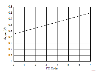
- 9.3.3 VO_REG and VIREG Calculations
- 9.3.4 RILIM Calculations
- 9.3.5 Adapter Enable Functionality
- 9.3.6 Turning Off the Transmitter
- 9.3.7 CM_ILIM
- 9.3.8 PD_DET and TMEM
- 9.3.9 TS, Both WPC and PMA
- 9.3.10 I2C Communication
- 9.3.11 Input Overvoltage
- 9.4 Device Functional Modes
- 9.5 Register Maps
-
10Application and Implementation
- 10.1 Application Information
- 10.2
Typical Applications
- 10.2.1
Dual Mode Design (WPC and PMA Compliant) Power Supply 5-V Output With 1-A Maximum Current
- 10.2.1.1 Design Requirements
- 10.2.1.2
Detailed Design Procedure
- 10.2.1.2.1 Output Voltage Set Point
- 10.2.1.2.2 Output and Rectifier Capacitors
- 10.2.1.2.3 Maximum Output Current Set Point
- 10.2.1.2.4 TERM Resistor
- 10.2.1.2.5 Setting LPRB1 and LPRB2 Resistors
- 10.2.1.2.6 I2C
- 10.2.1.2.7 Communication Current Limit
- 10.2.1.2.8 Receiver Coil
- 10.2.1.2.9 Series and Parallel Resonant Capacitors
- 10.2.1.2.10 Communication, Boot and Clamp Capacitors
- 10.2.1.3 Application Curves
- 10.2.2 bq51221 Embedded in System Board
- 10.2.3 bq51221 Implemented in Back Cover
- 10.2.1
Dual Mode Design (WPC and PMA Compliant) Power Supply 5-V Output With 1-A Maximum Current
- 11Power Supply Recommendations
- 12Layout
- 13Device and Documentation Support
- 14Mechanical, Packaging, and Orderable Information
Package Options
Mechanical Data (Package|Pins)
- YFP|42
Thermal pad, mechanical data (Package|Pins)
Orderable Information
8 Specifications
8.1 Absolute Maximum Ratings
over operating free-air temperature (unless otherwise noted)(1)(2)(1) All voltages are with respect to the PGND pin, unless otherwise noted.
(2) Stresses beyond those listed under absolute maximum ratings may cause permanent damage to the device. These are stress ratings only, and functional operation of the device at these or any other conditions beyond those indicated under recommended operating conditions is not implied. Exposure to absolute-maximum-rated conditions for extended periods may affect device reliability.
8.2 Handling Ratings
| MIN | MAX | UNIT | |||
|---|---|---|---|---|---|
| Tstg | Storage temperature | –65 | 150 | °C | |
| V(ESD)(1) | Electrostatic discharge | Human body model (HBM), per ANSI/ESDA/JEDEC JS-001, all pins(2), 100 pF, 1.5 kΩ | –2 | 2 | kV |
| Charged device model (CDM), per JEDEC specification JESD22-C101, all pins(3) | –500 | 500 | V | ||
(1) Electrostatic discharge (ESD) to measure device sensitivity and immunity to damage caused by assembly line electrostatic discharges in to the device.
(2) JEDEC document JEP155 states that 500-V HBM allows safe manufacturing with a standard ESD control process.
(3) JEDEC document JEP157 states that 250-V CDM allows safe manufacturing with a standard ESD control process.
8.3 Recommended Operating Conditions
over operating free-air temperature range (unless otherwise noted)| MIN | MAX | UNIT | ||
|---|---|---|---|---|
| VRECT | RECT voltage range | 4 | 10 | V |
| IOUT | Output current | 1 | A | |
| IAD-EN | Sink current | 1 | mA | |
| ICOMM | COMMx sink current | 500 | mA | |
| TJ | Junction temperature | 0 | 125 | ºC |
8.4 Thermal Information
| THERMAL METRIC(1) | bq51221 | UNIT | |
|---|---|---|---|
| YFP (42 Pins) | |||
| RθJA | Junction-to-ambient thermal resistance(2) | 49.7 | °C/W |
| RθJC(top) | Junction-to-case (top) thermal resistance(3) | 0.2 | |
| RθJB | Junction-to-board thermal resistance(4) | 6.1 | |
| ψJT | Junction-to-top characterization parameter(5) | 1.4 | |
| ψJB | Junction-to-board characterization parameter(6) | 6 | |
| RθJC(bot) | Junction-to-case (bottom) thermal resistance(7) | N/A | |
(1) For more information about traditional and new thermal metrics, see the IC Package Thermal Metrics application report, SPRA953.
(2) The junction-to-ambient thermal resistance under natural convection is obtained in a simulation on a JEDEC-standard, high-K board, as specified in JESD51-7, in an environment described in JESD51-2a.
(3) The junction-to-case (top) thermal resistance is obtained by simulating a cold plate test on the package top. No specific JEDEC-standard test exists, but a close description can be found in the ANSI SEMI standard G30-88.
(4) The junction-to-board thermal resistance is obtained by simulating in an environment with a ring cold plate fixture to control the PCB temperature, as described in JESD51-8.
(5) The junction-to-top characterization parameter, ψJT, estimates the junction temperature of a device in a real system and is extracted from the simulation data for obtaining RθJA, using a procedure described in JESD51-2a (sections 6 and 7).
(6) The junction-to-board characterization parameter, ψJB, estimates the junction temperature of a device in a real system and is extracted from the simulation data for obtaining RθJA, using a procedure described in JESD51-2a (sections 6 and 7).
(7) The junction-to-case (bottom) thermal resistance is obtained by simulating a cold plate test on the exposed (power) pad. No specific JEDEC standard test exists, but a close description can be found in the ANSI SEMI standard G30-88.
8.5 Electrical Characteristics
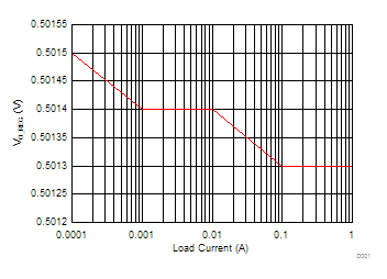
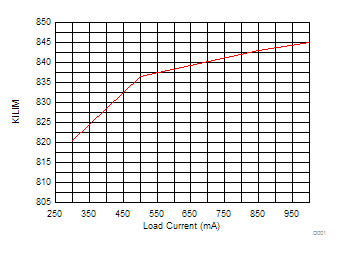
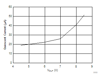
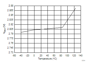
over operating free-air temperature range (unless otherwise noted), ILOAD = IOUT8.6 Typical Characteristics
Temperature = 25°C (unless otherwise noted)