SWAS031D June 2013 – February 2015 CC3100
PRODUCTION DATA.
- 1Device Overview
- 2Revision History
- 3Terminal Configuration and Functions
-
4Specifications
- 4.1 Absolute Maximum Ratings
- 4.2 Handling Ratings
- 4.3 Power-On Hours
- 4.4 Recommended Operating Conditions
- 4.5 Brown-Out and Black-Out
- 4.6 Electrical Characteristics (3.3 V, 25°C)
- 4.7 WLAN Receiver Characteristics
- 4.8 WLAN Transmitter Characteristics
- 4.9 Current Consumption
- 4.10 Thermal Characteristics for RGC Package
- 4.11 Timing and Switching Characteristics
- 4.12 External Interfaces
- 4.13 Host UART
- 5Detailed Description
- 6Applications and Implementation
- 7Device and Documentation Support
- 8Mechanical Packaging and Orderable Information
Package Options
Mechanical Data (Package|Pins)
- RGC|64
Thermal pad, mechanical data (Package|Pins)
- RGC|64
Orderable Information
4 Specifications
All measurements are referenced at the device pins, unless otherwise indicated. All specifications are over process and voltage, unless otherwise indicated.
4.1 Absolute Maximum Ratings
over operating free-air temperature range (unless otherwise noted)| PARAMETERS | PINS | MIN | MAX | UNIT |
|---|---|---|---|---|
| VBAT and VIO | 37, 39, 44 | –0.5 | 3.8 | V |
| VIO-VBAT (differential) | 10, 54 | 0.0 | V | |
| Digital inputs | –0.5 | VIO + 0.5 | V | |
| RF pins | –0.5 | 2.1 | V | |
| Analog pins (XTAL) | –0.5 | 2.1 | V | |
| Operating temperature range (TA ) | –40 | +85 | °C |
4.2 Handling Ratings
| MIN | MAX | UNIT | |||
|---|---|---|---|---|---|
| Tstg | Storage temperature range | –55 | +125 | °C | |
| VESD | Electrostatic discharge | Human body model (HBM), per ANSI/ESDA/JEDEC JS-001, all pins(1) | –2000 | +2000 | V |
| Charged device model (CDM), per JEDEC specification JESD22-C101, all pins(2) | –500 | +500 | V | ||
4.3 Power-On Hours
| CONDITIONS | POH | |
|---|---|---|
| TAmbient up to 85°C, assuming 20% active mode and 80% sleep mode | 17,500(1) | |
4.4 Recommended Operating Conditions
over operating free-air temperature range (unless otherwise noted) (1)(4)| PARAMETERS | PINS | CONDITIONS(2)(3) | MIN | TYP | MAX | UNIT |
|---|---|---|---|---|---|---|
| VBAT, VIO (shorted to VBAT) | 10, 37, 39, 44, 54 | Direct battery connection | 2.1 | 3.3 | 3.6 | V |
| VBAT, VIO (shorted to VBAT) | 10, 37, 39, 44, 54 | Preregulated 1.85 V | 1.76 | 1.85 | 1.9 | V |
| Ambient thermal slew | –20 | 20 | °C/minute |
4.5 Brown-Out and Black-Out
The device enters a brown-out condition whenever the input voltage dips below VBROWN (see Figure 4-1 and Figure 4-2). This condition must be considered during design of the power supply routing, especially if operating from a battery. High-current operations (such as a TX packet) cause a dip in the supply voltage, potentially triggering a brown-out. The resistance includes the internal resistance of the battery, contact resistance of the battery holder (4 contacts for a 2 x AA battery) and the wiring and PCB routing resistance.
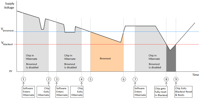 Figure 4-1 Brown-Out and Black-Out Levels (1 of 2)
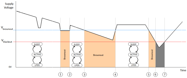 Figure 4-2 Brown-Out and Black-Out Levels (2 of 2)
In the brown-out condition, all sections of the device shut down except for the Hibernate module (including the 32-kHz RTC clock), which remains on. The current in this state can reach approximately 400 µA.
The black-out condition is equivalent to a hardware reset event in which all states within the device are lost.
Table 4-1 lists the brown-out and black-out voltage levels.
Table 4-1 Brown-Out and Black-out Voltage Levels
| CONDITION | VOLTAGE LEVEL | UNIT |
|---|---|---|
| Vbrownout | 2.1 | V |
| Vblackout | 1.67 | V |
4.6 Electrical Characteristics (3.3 V, 25°C)
| PARAMETER | TEST CONDITIONS | MIN | NOM | MAX | UNIT | ||
|---|---|---|---|---|---|---|---|
| CIN | Pin capacitance | 4 | pF | ||||
| VIH | High-level input voltage | 0.65 × VDD | VDD + 0.5 V | V | |||
| VIL | Low-level input voltage | –0.5 | 0.35 × VDD | V | |||
| IIH | High-level input current | 5 | nA | ||||
| IIL | Low-level input current | 5 | nA | ||||
| VOH | High-level output voltage (VDD = 3.0 V) |
2.4 | V | ||||
| VOL | Low-level output voltage (VDD = 3.0 V) |
0.4 | V | ||||
| IOH | High-level source current, VOH = 2.4 | 6 | mA | ||||
| IOL | Low-level sink current, VOH = 0.4 | 6 | mA | ||||
| Pin Internal Pullup and Pulldown (25°C) | |||||||
| PARAMETER | TEST CONDITIONS | MIN | NOM | MAX | UNIT | ||
| IOH | Pull-Up current, VOH = 2.4 (VDD = 3.0 V) |
5 | 10 | µA | |||
| IOL | Pull-Down current, VOL = 0.4 (VDD = 3.0 V) |
5 | µA | ||||
| VIL | nRESET(1) | 0.6 | V | ||||
4.7 WLAN Receiver Characteristics
TA = +25°C, VBAT = 2.1 to 3.6 V. Parameters measured at SoC pin on channel 7 (2442 MHz)| Parameter | Condition (Mbps) | Min | Typ | Max | Units |
|---|---|---|---|---|---|
| Sensitivity (8% PER for 11b rates, 10% PER for 11g/11n rates)(10% PER)(2) |
1 DSSS | –95.7 | dBm | ||
| 2 DSSS | –93.6 | ||||
| 11 CCK | –88.0 | ||||
| 6 OFDM | –90.0 | ||||
| 9 OFDM | –89.0 | ||||
| 18 OFDM | –86.0 | ||||
| 36 OFDM | –80.5 | ||||
| 54 OFDM | –74.0 | ||||
| MCS0 (GF)(1) | –89.0 | ||||
| MCS7 (GF)(1) | –71.0 | ||||
| Maximum input level (10% PER) |
802.11b | –4.0 | |||
| 802.11g | –10.0 |
4.8 WLAN Transmitter Characteristics
TA = +25°C, VBAT = 2.1 to 3.6 V. Parameters measured at SoC pin on channel 7 (2442 MHz).(1)| Parameter | Condition(2) | Min | Typ | Max | Units |
|---|---|---|---|---|---|
| Maximum RMS output power measured at 1 dB from IEEE spectral mask or EVM | 1 DSSS | 18.0 | dBm | ||
| 2 DSSS | 18.0 | ||||
| 11 CCK | 18.3 | ||||
| 6 OFDM | 17.3 | ||||
| 9 OFDM | 17.3 | ||||
| 18 OFDM | 17.0 | ||||
| 36 OFDM | 16.0 | ||||
| 54 OFDM | 14.5 | ||||
| MCS7 (MM) | 13.0 | ||||
| Transmit center frequency accuracy | –25 | 25 | ppm |
4.9 Current Consumption
TA = +25°C, VBAT = 3.6 V| PARAMETER | TEST CONDITIONS(1)(4) | MIN | TYP(5) | MAX | UNIT | ||||
|---|---|---|---|---|---|---|---|---|---|
| TX | 1 DSSS | TX power level = 0 | 272 | mA | |||||
| TX power level = 4 | 188 | ||||||||
| 6 OFDM | TX power level = 0 | 248 | |||||||
| TX power level = 4 | 179 | ||||||||
| 54 OFDM | TX power level = 0 | 223 | |||||||
| TX power level = 4 | 160 | ||||||||
| RX(7) | 1 DSSS | 53 | |||||||
| 54 OFDM | 53 | ||||||||
| Idle connected(2) | 0.690 | ||||||||
| LPDS | 0.115 | ||||||||
| Hibernate(6) | 4 | µA | |||||||
| Peak calibration current (3)(7) | VBAT = 3.3 V | 450 | mA | ||||||
| VBAT = 2.1 V | 670 | ||||||||
| VBAT = 1.85 V | 700 | ||||||||
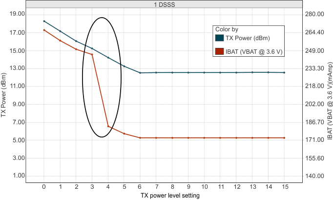
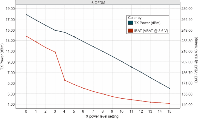 Figure 4-4 TX Power and IBAT vs TX Power Level Settings (6 OFDM)
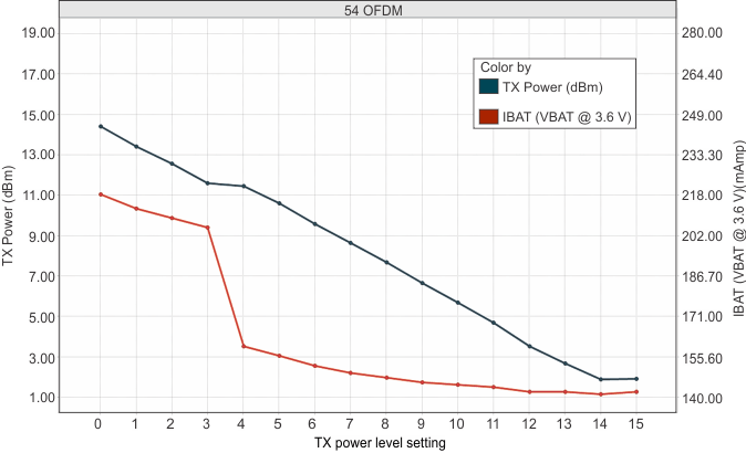 Figure 4-5 TX Power and IBAT vs TX Power Level Settings (54 OFDM)
4.10 Thermal Characteristics for RGC Package
| AIR FLOW | ||||
|---|---|---|---|---|
| PARAMETER | 0 lfm (C/W) | 150 lfm (C/W) | 250 lfm (C/W) | 500 lfm (C/W) |
| θja | 23 | 14.6 | 12.4 | 10.8 |
| Ψjt | 0.2 | 0.2 | 0.3 | 0.1 |
| Ψjb | 2.3 | 2.3 | 2.2 | 2.4 |
| θjc | 6.3 | |||
| θjb | 2.4 | |||
4.11 Timing and Switching Characteristics
4.11.1 Power Supply Sequencing
For proper operation of the CC3100 device, perform the recommended power-up sequencing as follows:
- Tie VBAT (pins 37, 39, 44) and VIO (pins 54 and 10) together on the board.
- Hold the RESET pin low while the supplies are ramping up. TI recommends using a simple RC circuit (100K || 0.1 µF, RC = 10 ms).
- For an external RTC clock, ensure that the clock is stable before RESET is deasserted (high).
For timing diagrams, see Section 4.11.2, Reset Timing.
4.11.2 Reset Timing
4.11.2.1 nRESET (32K XTAL)
Figure 4-6 shows the reset timing diagram for the 32K XTAL first-time power-up and reset removal.
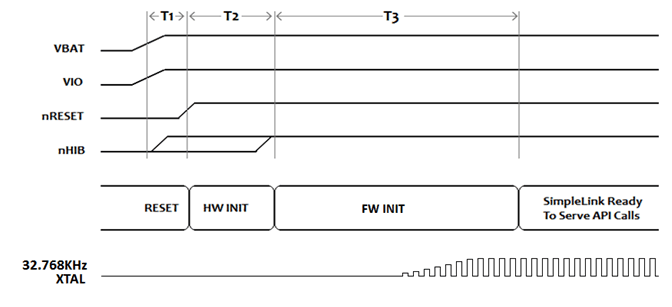 Figure 4-6 First-Time Power-Up and Reset Removal Timing Diagram (32K XTAL)
Table 4-2 describes the timing requirements for the 32K XTAL first-time power-up and reset removal.
Table 4-2 First-Time Power-Up and Reset Removal Timing Requirements (32K XTAL)
| Item | Name | Description | Min | Typ | Max |
|---|---|---|---|---|---|
| T1 | Supply settling time | Depends on application board power supply, decap, and so on | 3 ms | ||
| T2 | Hardware wakeup time | 25 ms | |||
| T3 | Initialization time | 32-kHz XTAL settling + firmware initialization time + radio calibration | 1.35 s |
4.11.2.2 nRESET (External 32K)
Figure 4-7 shows the reset timing diagram for the external 32K first-time power-up and reset removal.
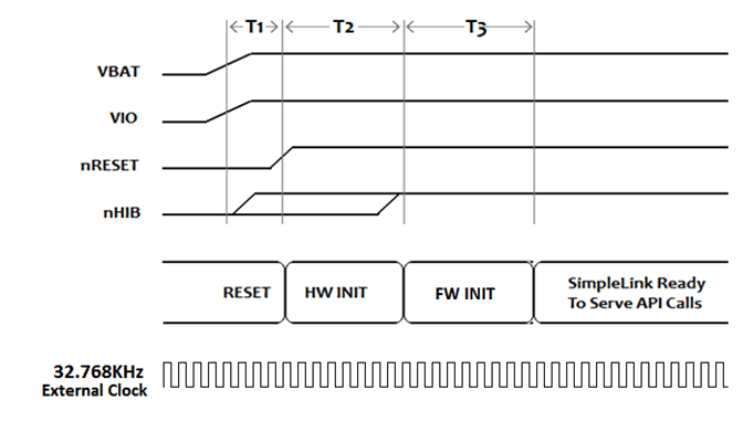 Figure 4-7 First-Time Power-Up and Reset Removal Timing Diagram (External 32K)
Table 4-3 describes the timing requirements for the external 32K first-time power-up and reset removal.
Table 4-3 First-Time Power-Up and Reset Removal Timing Requirements (External 32K)
| Item | Name | Description | Min | Typ | Max |
|---|---|---|---|---|---|
| T1 | Supply settling time | Depends on application board power supply, decap, and so on | 3 ms | ||
| T2 | Hardware wakeup time | 25 ms | |||
| T3 | Initialization time | Firmware initialization time + radio calibration | 250 ms |
4.11.2.3 Wakeup from Hibernate
Figure 4-8 shows the timing diagram for wakeup from the hibernate state.
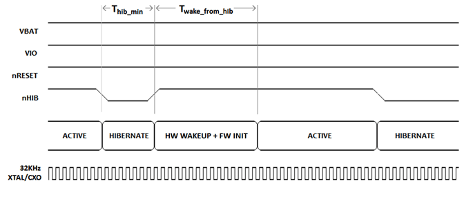 Figure 4-8 nHIB Timing Diagram
NOTE
The 32.768-kHz XTAL is kept enabled by default when the chip goes to hibernate in response to nHIB being pulled low.
Table 4-4 describes the timing requirements for nHIB.
Table 4-4 nHIB Timing Requirements
| Item | Name | Description | Min | Typ | Max |
|---|---|---|---|---|---|
| Thib_min | Minimum hibernate time | Minimum pulse width of nHIB being low(2) | 10 ms | ||
| Twake_from_hib | Hardware wakeup time plus firmware initialization time | See (1). | 50 ms |
4.11.3 Clock Specifications
The CC3100 device requires two separate clocks for its operation:
- A slow clock running at 32.768 kHz is used for the RTC.
- A fast clock running at 40 MHz is used by the device for the internal processor and the WLAN subsystem.
The device features internal oscillators that enable the use of cheaper crystals rather than dedicated TCXOs for these clocks. The RTC can also be fed externally to provide reuse of an existing clock on the system and reduce overall cost.
4.11.3.1 Slow Clock Using Internal Oscillator
The RTC crystal connected on the device supplies the free-running slow clock. The accuracy of the slow clock frequency must be 32.768 kHz ±150 ppm. In this mode of operation, the crystal is tied between RTC_XTAL_P (pin 51) and RTC_XTAL_N (pin 52) with a suitable load capacitance.
Figure 4-9 shows the crystal connections for the slow clock.
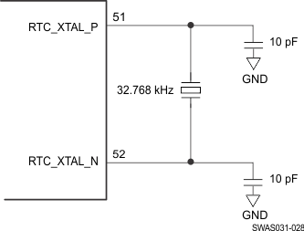 Figure 4-9 RTC Crystal Connections
4.11.3.2 Slow Clock Using an External Clock
When an RTC clock oscillator is present in the system, the CC3100 device can accept this clock directly as an input. The clock is fed on the RTC_XTAL_P line and the RTC_XTAL_N line is held to VIO. The clock must be a CMOS-level clock compatible with VIO fed to the device.
Figure 4-10 shows the external RTC clock input connection.
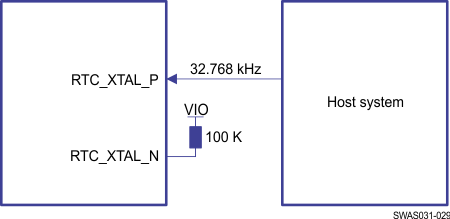 Figure 4-10 External RTC Clock Input
4.11.3.3 Fast Clock (Fref) Using an External Crystal
The CC3100 device also incorporates an internal crystal oscillator to support a crystal-based fast clock. The XTAL is fed directly between WLAN_XTAL_P (pin 23) and WLAN_XTAL_N (pin 22) with suitable loading capacitors.
Figure 4-11 shows the crystal connections for the fast clock.
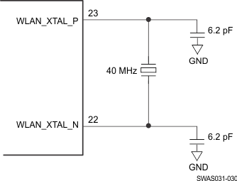 Figure 4-11 Fast Clock Crystal Connections
4.11.3.4 Fast Clock (Fref) Using an External Oscillator
The CC3100 device can accept an external TCXO/XO for the 40-MHz clock. In this mode of operation, the clock is connected to WLAN_XTAL_P (pin 23). WLAN_XTAL_N (pin 22) is connected to GND. The external TCXO/XO can be enabled by TCXO_EN (pin 21) from the device to optimize the power consumption of the system.
If the TCXO does not have an enable input, an external LDO with an enable function can be used. Using the LDO improves noise on the TCXO power supply.
Figure 4-12 shows the connection.
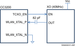 Figure 4-12 External TCXO Input
Table 4-5 lists the external Fref clock requirements.
Table 4-5 External Fref Clock Requirements (–40°C to +85°C)
| Characteristics | Condition | Sym | Min | Typ | Max | Unit | |
|---|---|---|---|---|---|---|---|
| Frequency | 40.00 | MHz | |||||
| Frequency accuracy (Initial + temp + aging) | ±25 | ppm | |||||
| Frequency input duty cycle | 45 | 50 | 55 | % | |||
| Clock voltage limits | Sine or clipped sine wave, AC coupled | Vpp | 0.7 | 1.2 | Vpp | ||
| Phase noise @ 40 MHz | @ 1 kHz | –125 | dBc/Hz | ||||
| @ 10 kHz | –138.5 | dBc/Hz | |||||
| @ 100 kHz | –143 | dBc/Hz | |||||
| Input impedance | Resistance | 12 | KΩ | ||||
| Capacitance | 7 | pF | |||||
4.11.3.5 Input Clocks/Oscillators
Table 4-6 lists the RTC crystal requirements.
Table 4-6 RTC Crystal Requirements
| CHARACTERISTICS | CONDITION | SYM | MIN | TYP | MAX | UNIT |
|---|---|---|---|---|---|---|
| Frequency | 32.768 | kHz | ||||
| Frequency accuracy | Initial + temp + aging | ±150 | ppm | |||
| Crystal ESR | 32.768 kHz, C1 = C2 = 10 pF | 70 | kΩ |
Table 4-7 lists the external RTC digital clock requirements.
Table 4-7 External RTC Digital Clock Requirements
| CHARACTERISTICS | CONDITION | SYM | MIN | TYP | MAX | UNIT |
|---|---|---|---|---|---|---|
| Frequency | 32768 | Hz | ||||
| Frequency accuracy | ±150 | ppm | ||||
| (Initial + temp + aging) | ||||||
| Input transition time tr/tf (10% to 90%) | tr/tf | 100 | ns | |||
| Frequency input duty cycle | 20 | 50 | 80 | % | ||
| Slow clock input voltage limits | Square wave, DC coupled | Vih | 0.65 × VIO | VIO | V | |
| Vil | 0 | 0.35 × VIO | V peak | |||
| Input impedance | 1 | MΩ | ||||
| 5 | pF |
Table 4-8 lists the WLAN fast-clock crystal requirements.
Table 4-8 WLAN Fast-Clock Crystal Requirements
| CHARACTERISTICS | CONDITION | SYM | MIN | TYP | MAX | UNIT |
|---|---|---|---|---|---|---|
| Frequency | 40 | MHz | ||||
| Frequency accuracy | Initial + temp + aging | ±25 | ppm | |||
| Crystal ESR | 40 MHz, C1 = C2 = 6.2 pF | 40 | 50 | 60 | Ohm |
4.11.3.6 WLAN Filter Requirements
The device requires an external bandpass filter to meet the various emission standards, including FCC. Table 4-9 presents the attenuation requirements for the bandpass filter. TI recommends using the same filter used in the reference design to ease the process of certification.
Table 4-9 WLAN Filter Requirements
| Parameter | Frequency (MHz) | Requirements | |||
|---|---|---|---|---|---|
| Min | Typ | Max | Units | ||
| Return loss | 2412 to 2484 | 10 | dB | ||
| Insertion loss(1) | 2412 to 2484 | 1 | 1.5 | dB | |
| Attenuation | 800 to 830 | 30 | 45 | dB | |
| 1600 to 1670 | 20 | 25 | |||
| 3200 to 3300 | 30 | 48 | |||
| 4000 to 4150 | 45 | 50 | |||
| 4800 to 5000 | 20 | 25 | |||
| 5600 to 5800 | 20 | 25 | |||
| 6400 to 6600 | 20 | 35 | |||
| 7200 to 7500 | 35 | 45 | |||
| 7500 to 10000 | 20 | 25 | |||
| Reference Impendence | 2412 to 2484 | 50 | Ω | ||
| Filter type | Bandpass | ||||
4.11.4 Interfaces
This section describes the interfaces that are supported by the CC3100 device:
- Host SPI
- Flash SPI
- Host UART
4.11.4.1 Host SPI Interface Timing
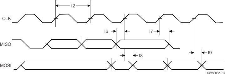 Figure 4-13 Host SPI Interface Timing
Table 4-10 Host SPI Interface Timing Parameters
| Parameter Number | Parameter(1) | Parameter Name | Min | Max | Unit |
|---|---|---|---|---|---|
| I1 | F | Clock frequency @ VBAT = 3.3 V | 20 | MHz | |
| Clock frequency @ VBAT ≤ 2.1 V | 12 | ||||
| I2 | tclk(2) | Clock period | 50 | ns | |
| I3 | tLP | Clock low period | 25 | ns | |
| I4 | tHT | Clock high period | 25 | ns | |
| I5 | D | Duty cycle | 45 | 55 | % |
| I6 | tIS | RX data setup time | 4 | ns | |
| I7 | tIH | RX data hold time | 4 | ns | |
| I8 | tOD | TX data output delay | 20 | ||
| I9 | tOH | TX data hold time | 24 | ns |
4.11.4.2 Flash SPI Interface Timing
Figure 4-14 Flash SPI Interface Timing
Table 4-11 Flash SPI Interface Timing Parameters
4.12 External Interfaces
4.12.1 SPI Flash Interface
The external serial flash stores the user profiles and firmware patch updates. The CC3100 device acts as a master in this case; the SPI serial flash acts as the slave device. This interface can work up to a speed of 20 MHz.
Figure 4-15 shows the SPI flash interface.
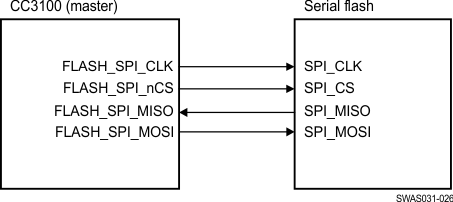 Figure 4-15 SPI Flash Interface
Table 4-12 lists the SPI flash interface pins.
4.12.2 SPI Host Interface
The device interfaces to an external host using the SPI interface. The CC3100 device can interrupt the host using the HOST_INTR line to initiate the data transfer over the interface. The SPI host interface can work up to a speed of 20 MHz.
Figure 4-16 shows the SPI host interface.
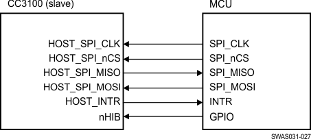 Figure 4-16 SPI Host Interface
Table 4-13 lists the SPI host interface pins.
Table 4-13 SPI Host Interface
| Pin Name | Description |
|---|---|
| HOST_SPI_CLK | Clock (up to 20 MHz) from MCU host to CC3100 device |
| HOST_SPI_nCS | CS (active low) signal from MCU host to CC3100 device |
| HOST_SPI_MOSI | Data from MCU host to CC3100 device |
| HOST_INTR | Interrupt from CC3100 device to MCU host |
| HOST_SPI_MISO | Data from CC3100 device to MCU host |
| nHIB | Active-low signal that commands the CC3100 device to enter hibernate mode (lowest power state) |
4.13 Host UART
The SimpleLink device requires the UART configuration described in Table 4-14.
Table 4-14 SimpleLink UART Configuration
| Property | Supported CC3100 Configuration |
|---|---|
| Baud rate | 115200 bps, no auto-baud rate detection, can be changed by the host up to 3 Mbps using a special command |
| Data bits | 8 bits |
| Flow control | CTS/RTS |
| Parity | None |
| Stop bits | 1 |
| Bit order | LSBit first |
| Host interrupt polarity | Active high |
| Host interrupt mode | Rising edge or level 1 |
| Endianness | Little-endian only(1) |
4.13.1 5-Wire UART Topology
Figure 4-17 shows the typical 5-wire UART topology comprised of 4 standard UART lines plus one IRQ line from the device to the host controller to allow efficient low power mode.
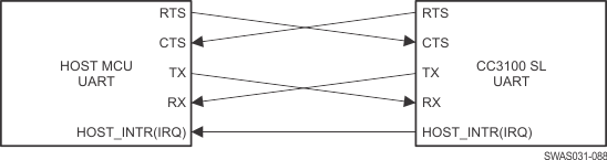
This is the typical and recommended UART topology because it offers the maximum communication reliability and flexibility between the host and the SimpleLink device.
4.13.2 4-Wire UART Topology
The 4-wire UART topology eliminates the host IRQ line (see Figure 4-18). Using this topology requires one of the following conditions to be met:
- Host is always awake or active.
- Host goes to sleep but the UART module has receiver start-edge detection for auto wakeup and does not lose data.
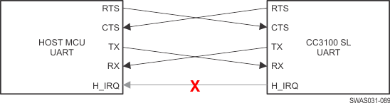 Figure 4-18 4-Wire UART Configuration
4.13.3 3-Wire UART Topology
The 3-wire UART topology requires only the following lines (see Figure 4-19):
- RX
- TX
- CTS
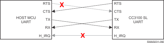 Figure 4-19 3-Wire UART Topology
Using this topology requires one of the following conditions to be met:
- Host always stays awake or active.
- Host goes to sleep but the UART module has receiver start-edge detection for auto wakeup and does not lose data.
- Host can always receive any amount of data transmitted by the SimpleLink device because there is no flow control in this direction.
Because there is no full flow control, the host cannot stop the SimpleLink device to send its data; thus, the following parameters must be carefully considered:
- Max baud rate
- RX character interrupt latency and low-level driver jitter buffer
- Time consumed by the user's application