SWAS032F July 2013 – February 2015 CC3200
PRODUCTION DATA.
- 1Device Overview
- 2Revision History
- 3Terminal Configuration and Functions
-
4Specifications
- 4.1 Absolute Maximum Ratings
- 4.2 Handling Ratings
- 4.3 Power-On Hours
- 4.4 Recommended Operating Conditions
- 4.5 Brown-Out and Black-Out
- 4.6 Electrical Characteristics (3.3 V, 25°C)
- 4.7 WLAN Receiver Characteristics
- 4.8 WLAN Transmitter Characteristics
- 4.9 Current Consumption
- 4.10 Thermal Characteristics for RGC Package
- 4.11 Timing and Switching Characteristics
- 5Detailed Description
- 6Applications and Implementation
- 7Device and Documentation Support
- 8Mechanical Packaging and Orderable Information
Package Options
Mechanical Data (Package|Pins)
- RGC|64
Thermal pad, mechanical data (Package|Pins)
- RGC|64
Orderable Information
6 Applications and Implementation
6.1 Application Information
6.1.1 Typical Application – CC3200 Wide-Voltage Mode
Figure 6-1 shows the schematics for an application using the CC3200 wide-voltage mode.
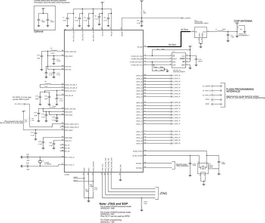
NOTE: This schematic is rated from 2.3 to 3.6 V because of the limitation of the serial flash.
Figure 6-1 Schematics for CC3200 Wide-Voltage Mode Application
Table 6-1 lists the bill of materials for an application using the CC3200 wide-voltage mode.
Table 6-1 Bill of Materials for CC3200 Wide-Voltage Mode Application
| Item | Qty | Part Reference | Value | Manufacturer | Part Number | Description |
|---|---|---|---|---|---|---|
| 1 | 3 | C1 C2 C3 | 4.7 µF | Samsung Electro-Mechanics America, Inc | CL05A475MQ5NRNC | Capacitor, Ceramic: 4.7 µF 6.3 V 20% X5R 0402 |
| 2 | 13 | C4 C5 C8 C11 C12 C13 C14 C17 C19 C20 C21 C22 C23 | 0.1 µF | Taiyo Yuden | LMK105BJ104KV-F | Capacitor, Ceramic: 0.1 µF 10 V 10% X5R 0402 |
| 3 | 1 | C9 | 1.0 pF | Murata Electronics North America | GJM1555C1H1R0BB01D | Capacitor, Ceramic: 1 pF 50 V NP0 0402 |
| 4 | 2 | C10 C18 | 10 µF | Murata Electronics North America | GRM188R60J106ME47D | Capacitor, Ceramic: 10 µF 6.3 V 20% X5R 0603 |
| 5 | 2 | C15 C16 | 22 µF | Taiyo Yuden | AMK107BBJ226MAHT | Capacitor, Ceramic: 22 µF 4 V 20% X5R 0603 |
| 6 | 2 | C24 C46 | 10 pF | Murata Electronics North America | GRM1555C1H100FA01D | Capacitor, Ceramic: 10 pF 50 V 1% NP0 0402 |
| 7 | 2 | C42 C49 | 6.2 pF | Murata Electronics North America | GRM1555C1H6R2BA01D | Capacitor, Ceramic: 6.2 pF 50 V NP0 0402 |
| 8 | 1 | E2 | 2.4-GHz Ant | Taiyo Yuden | AH316M245001-T | Chip Antenna: 50 Ω Bluetooth WLAN ZigBee® WIMAX |
| 9 | 1 | FL1 | 2.4-GHz Filter | TDK-Epcos | DEA202450BT-1294C1-H | Filter, Bandpass: 2.4 GHz WLAN SMD |
| 10 | 1 | L1 | 3.6 nH | Murata Electronics North America | LQP15MN3N6B02D | Inductor: 3.6 nH 0.1 nH 0402 |
| 11 | 2 | L2 L8 | 2.2 µH | Murata Electronics North America | LQM2HPN2R2MG0L | Inductor: 2.2 µH 20% 1300 mA 1008 |
| 12 | 1 | L3 | 1 µH | Murata | LQM2HPN1R0MJ0L | Inductor, Power: 1.0 µH 1500 mA 1007 |
| 16 | 1 | U1 | 8M (1M x 8) |
Micron Technology Inc | M25PX80-VMN6TP | IC Flash: 8Mb 75 MHz 8SO |
| 17 | 1 | U2 | CC3200 | Texas Instruments | CC3200R1 | ARM M4 MCU with 802.11bgn WI-FI |
| 18 | 1 | Y1 | Crystal | Abracon Corporation | ABS07-32.768KHZ-T | Crystal: 32.768 kHz 12.5 pF SMD |
| 19 | 1 | Y2 | Crystal | Epson | Q24FA20H00396 | Crystal: 40 MHz 8 pF SMD |
NOTE
Use any 5% tolerance resistor 0402 or higher package.
6.1.2 Typical Application – CC3200 Preregulated 1.85-V Mode
Figure 6-2 shows the schematics for an application using the CC3200 preregulated 1.85-V mode.
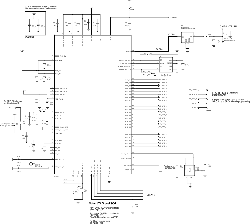
Table 6-1 lists the bill of materials for an application using the CC3200 preregulated 1.85-V mode.
Table 6-2 Bill of Materials for CC3200 Preregulated 1.85-V Mode Application
| Item | Qty | Part Reference | Value | Manufacturer | Part Number | Description |
|---|---|---|---|---|---|---|
| 1 | 3 | C1 C2 C3 | 4.7 µF | Samsung Electro-Mechanics America, Inc | CL05A475MQ5NRNC | Capacitor, Ceramic: 4.7 µF 6.3 V 20% X5R 0402 |
| 2 | 12 | C4 C5 C8 C11 C12 C14 C17 C19 C20 C21 C22 C23 | 0.1 µF | Taiyo Yuden | LMK105BJ104KV-F | Capacitor, Ceramic: 0.1 µF 10 V 10% X5R 0402 |
| 3 | 1 | C9 | 1.0 pF | Murata Electronics North America | GJM1555C1H1R0BB01D | Capacitor, Ceramic: 1 pF 50 V NP0 0402 |
| 4 | 1 | C16 | 22 µF | Taiyo Yuden | AMK107BBJ226MAHT | Capacitor, Ceramic: µF 4 V 20% X5R 0603 |
| 5 | 2 | C13 C18 | 10 µF | Murata Electronics North America | GRM188R60J106ME47D | Capacitor, Ceramic: 10 µF 6.3 V 20% X5R 0603 |
| 6 | 2 | C24 C46 | 10 pF | Murata Electronics North America | GRM1555C1H100FA01D | Capacitor, Ceramic: 10 pF 50 V 1% NP0 0402 |
| 7 | 2 | C42 C49 | 6.2 pF | Murata Electronics North America | GRM1555C1H6R2BA01D | Capacitor, Ceramic: 6.2 pF 50 V NP0 0402 |
| 8 | 1 | E2 | 2.4-GHz Ant | Taiyo Yuden | AH316M245001-T | Antenna, Chip: 50 Ω Bluetooth WLAN ZigBee WIMAX |
| 9 | 1 | FL1 | 2.4-GHz Filter | TDK-Epcos | DEA202450BT-1294C1-H | Filter, Bandpass: 2.4 GHz WLAN SMD |
| 10 | 1 | L1 | 3.6 nH | Murata Electronics North America | LQP15MN3N6B02D | Inductor: 3.6 nH 0.1 nH 0402 |
| 11 | 1 | L8 | 2.2 µH | Murata Electronics North America | LQM2HPN2R2MG0L | Inductor: 2.2 µH 20% 1300 mA 1008 |
| 15 | 1 | U1 | 8M (1M x 8) |
Winbond | W25Q80BWZPIG | IC FLASH 8Mb 75 MHz 8WSON |
| 16 | 1 | U2 | CC3200 | Texas Instruments | CC3200R1 | ARM M4 MCU with 802.11bgn WIFI |
| 17 | 1 | Y1 | Crystal | Abracon Corporation | ABS07-32.768KHZ-T | Crystal: 32.768 kHz 12.5 pF SMD |
| 18 | 1 | Y2 | Crystal | Epson | Q24FA20H00396 | Crystal: 40 MHz 8 pF SMD |
NOTE
Use any 5% tolerance resistor 0402 or higher package.