SCAS666D June 2001 – October 2015 CDCVF2310
PRODUCTION DATA.
- 1 Features
- 2 Applications
- 3 Description
- 4 Revision History
- 5 Pin Configuration and Functions
- 6 Specifications
- 7 Parameter Measurement Information
- 8 Detailed Description
- 9 Application and Implementation
- 10Power Supply Recommendations
- 11Layout
- 12Device and Documentation Support
- 13Mechanical, Packaging, and Orderable Information
Package Options
Refer to the PDF data sheet for device specific package drawings
Mechanical Data (Package|Pins)
- PW|24
Thermal pad, mechanical data (Package|Pins)
Orderable Information
1 Features
- High-Performance 1:10 Clock Driver
- Operates up to 200 MHz at VDD 3.3 V
- Pin-to-Pin Skew < 100 ps at VDD 3.3 V
- VDD Range: 2.3 V to 3.6 V
- Operating Temperature Range –40°C to 105°C
- Supports 105ºC Ambient Temperature (see Thermal Considerations)
- Output Enable Glitch Suppression
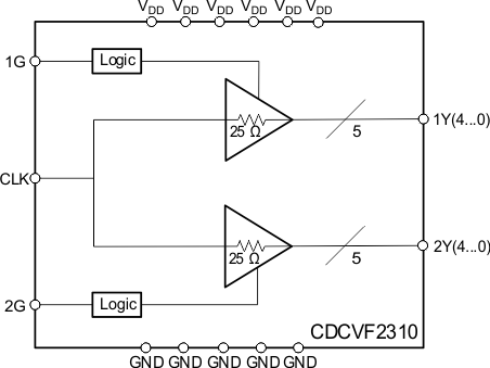
- Distributes One Clock Input to Two Banks of Five Outputs
- 25-Ω On-Chip Series Damping Resistors
- Packaged in 24-Pin TSSOP
2 Applications
- General-Purpose Applications
3 Description
The CDCVF2310 device is a high-performance, low-skew clock buffer that operates up to 200 MHz. Two banks of five outputs each provide low-skew copies of CLK. After power up, the default state of the outputs is low regardless of the state of the control pins. For normal operation, the outputs of bank 1Y[0:4] or 2Y[0:4] can be placed in a low state when the control pins (1G or 2G, respectively) are held low and a negative clock edge is detected on the CLK input. The outputs of bank 1Y[0:4] or 2Y[0:4] can be switched into the buffer mode when the control pins (1G and 2G) are held high and a negative clock edge is detected on the CLK input. The device operates in a 2.5-V and 3.3-V environment. The built-in output enable glitch suppression ensures a synchronized output enable sequence to distribute full period clock signals.
The CDCVF2310 is characterized for operation from –40°C to 85°C.
Device Information (1)
| PART NUMBER | PACKAGE | BODY SIZE (NOM) |
|---|---|---|
| CDCVF2310 | TSSOP (24) | 4.40 mm × 7.80 mm |
- For all available packages, see the orderable addendum at the end of the data sheet.
Functional Block Diagram
