SLPS667A February 2017 – July 2017 CSD17318Q2
PRODUCTION DATA.
- 1Features
- 2Applications
- 3Description
- 4Revision History
- 5Specifications
- 6Device and Documentation Support
- 7Mechanical Data
Package Options
Refer to the PDF data sheet for device specific package drawings
Mechanical Data (Package|Pins)
- DQK|6
Thermal pad, mechanical data (Package|Pins)
Orderable Information
7 Mechanical Data
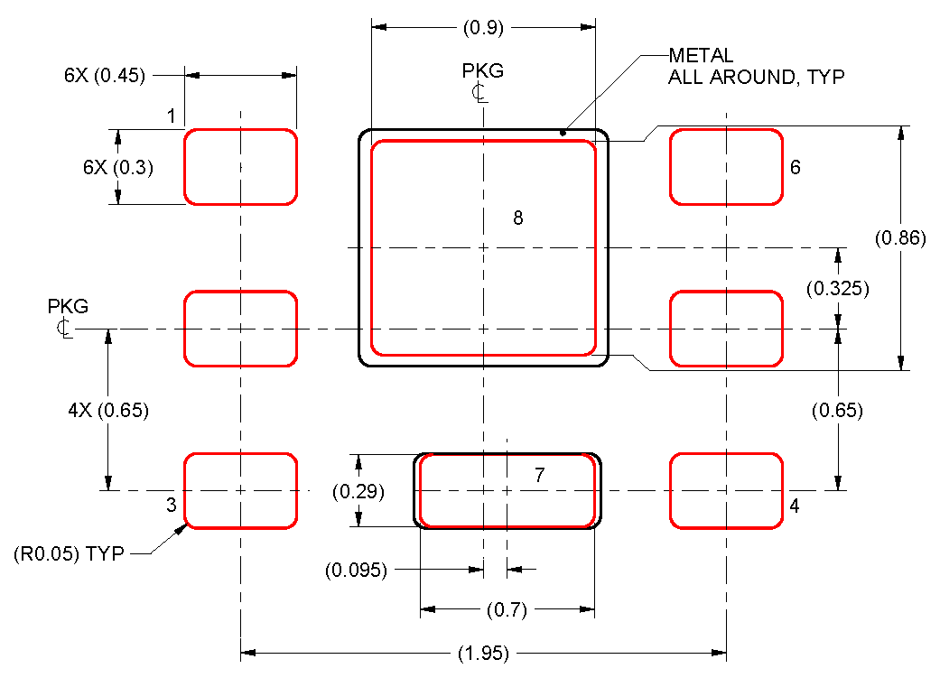
7.1 Q2 Package Dimensions

- All linear dimensions are in millimeters. Any dimensions in parenthesis are for reference only. Dimensioning and tolerancing per ASME Y14.5M.
- This drawing is subject to change without notice.
- The package thermal pads must be soldered to the printed circuit board for thermal and mechanical performance.
7.1.1 Recommended PCB Pattern


- This package is designed to be soldered to a thermal pad on the board. For more information, see QFN/SON PCB Attachment (SLUA271).
7.1.2 Recommended Stencil Pattern

- Laser cutting apertures with trapezoidal walls and rounded corners may offer better paste release. IPC-7525 may have alternate design recommendations.
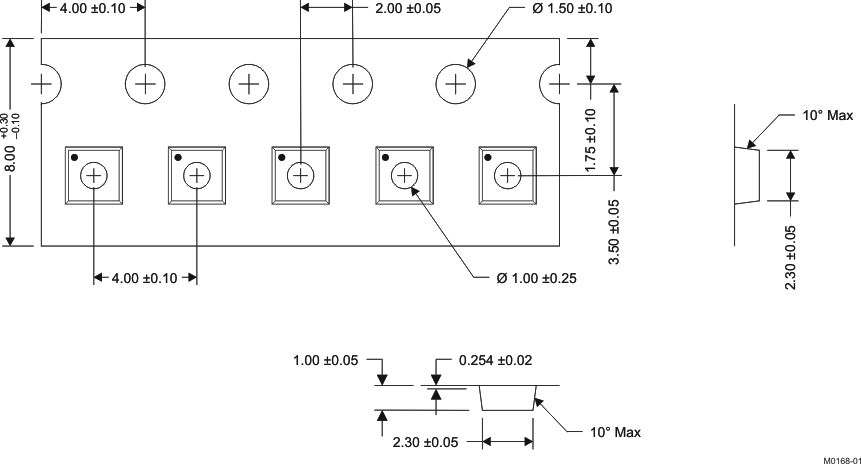
7.2 Q2 Tape and Reel Information

NOTES:
1. Measured from centerline of sprocket hole to centerline of pocket.2. Cumulative tolerance of 10 sprocket holes is ±0.20.
3. Other material available.
4. Typical SR of form tape Max 109 OHM/SQ.
5. All dimensions are in mm, unless otherwise specified.