SLPS459A January 2014 – June 2014 CSD25310Q2
PRODUCTION DATA.
- 1Features
- 2Applications
- 3Description
- 4Revision History
- 5Specifications
- 6Device and Documentation Support
- 7Mechanical, Packaging, and Orderable Information
Package Options
Refer to the PDF data sheet for device specific package drawings
Mechanical Data (Package|Pins)
- DQK|6
Thermal pad, mechanical data (Package|Pins)
Orderable Information
1 Features
2 Applications
- Battery Management
- Load Management
- Battery Protection
3 Description
This 19.9 mΩ, –20 V P-Channel device is designed to deliver the lowest on resistance and gate charge in the smallest outline possible with excellent thermal characteristics in an ultra-low profile. Its low on resistance coupled with an extremely small footprint in a SON 2 mm × 2 mm plastic package make the device ideal for battery operated space constrained operations.
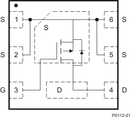
Top View
Product Summary
| TA = 25°C | TYPICAL VALUE | UNIT | ||
|---|---|---|---|---|
| VDS | Drain-to-Source Voltage | –20 | V | |
| Qg | Gate Charge Total (–4.5 V) | 3.6 | nC | |
| Qgd | Gate Charge Gate to Drain | 0.5 | nC | |
| RDS(on) | Drain-to-Source On Resistance | VGS = –1.8 V | 59.0 | mΩ |
| VGS = –2.5 V | 27.0 | mΩ | ||
| VGS = –4.5 V | 19.9 | mΩ | ||
| VGS(th) | Threshold Voltage | -0.85 | V | |
Ordering Information(1)
| Device | Media | Qty | Package | Ship |
|---|---|---|---|---|
| CSD25310Q2 | 7-Inch Reel | 3000 | SON 2 x 2 mm Plastic Package |
Tape and Reel |
| CSD25310Q2T | 7-Inch Reel | 250 |
- For all available packages, see the orderable addendum at the end of the data sheet.
Absolute Maximum Ratings
| TA = 25°C | VALUE | UNIT | |
|---|---|---|---|
| VDS | Drain-to-Source Voltage | –20 | V |
| VGS | Gate-to-Source Voltage | ±8 | V |
| ID | Continuous Drain Current (Package Limit) | –20 | A |
| Continuous Drain Current(1) | –9.6 | A | |
| IDM | Pulsed Drain Current(2) | 48 | A |
| PD | Power Dissipation(1) | 2.9 | W |
| TJ, Tstg | Operating Junction and Storage Temperature Range | –55 to 150 | °C |
- RθJA = 43°C/W on 1 in² Cu (2 oz.) on .060-inch thick FR4 PCB.
- Pulse duration 10 μs, duty cycle ≤2%
RDS(on) vs VGS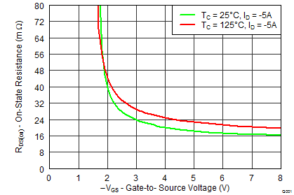 |
Gate Charge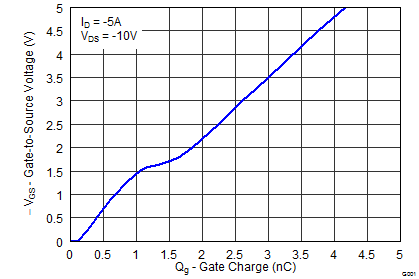 |