SLPS661 September 2017 CSD87503Q3E
PRODUCTION DATA.
- 1Features
- 2Applications
- 3Description
- 4Revision History
- 5 Specifications
- 6Device and Documentation Support
- 7Mechanical, Packaging, and Orderable Information
Package Options
Mechanical Data (Package|Pins)
- DTD|8
Thermal pad, mechanical data (Package|Pins)
Orderable Information
1 Features
- Dual N-Ch Common Source MOSFETs
- Optimized for 5-V Gate Drive
- Low-Thermal Resistance
- Low Qg and Qgd
- Lead-Free Terminal Plating
- RoHS Compliant
- Halogen Free
- SON 3.3-mm × 3.3-mm Plastic Package
2 Applications
- USB Type-C/PD VBus Protection
- Battery Protection
- Load Switch
3 Description
The CSD87503Q3E is a 30-V, 13.5-mΩ, common source, dual N-channel device designed for USB Type-C/PD and battery protection. This SON 3.3 × 3.3 mm device has low drain-to-drain on-resistance that minimizes losses and offers low component count for space constrained applications.
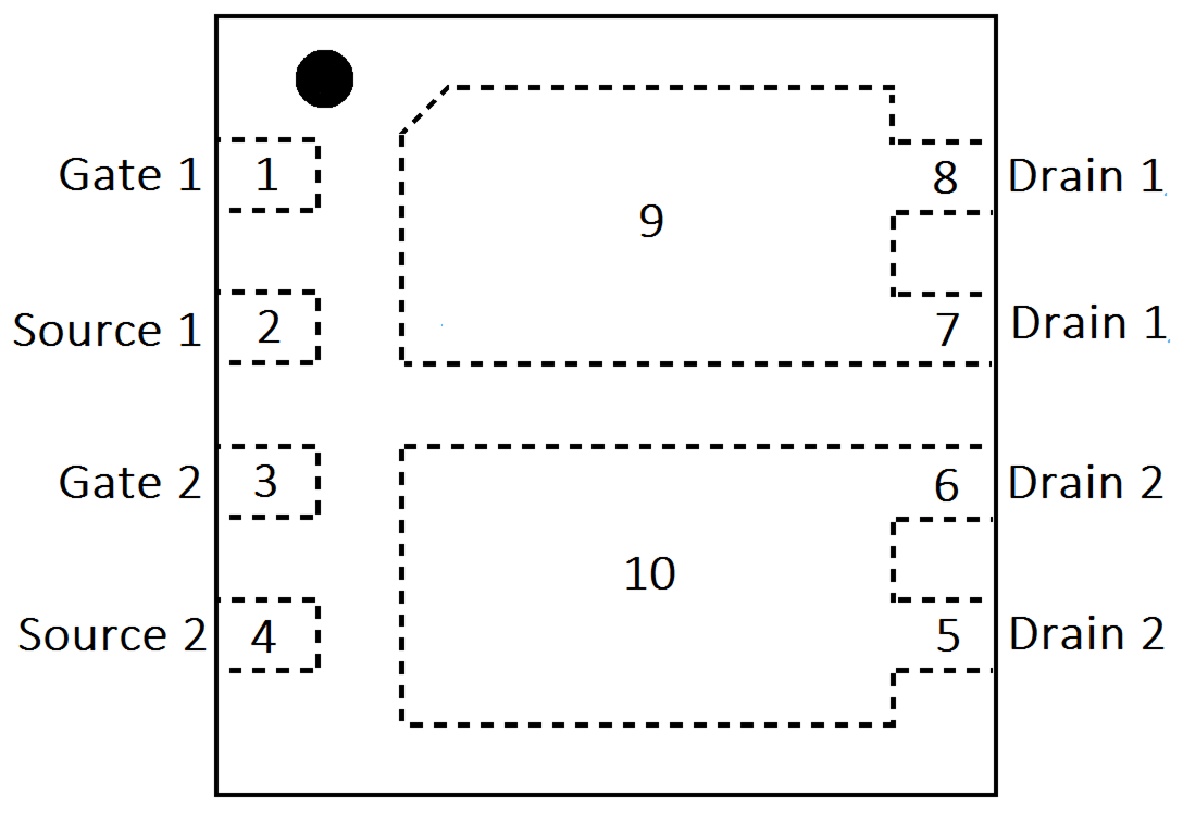
Top View

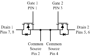
Circuit Image

Product Summary
| TA = 25°C | VALUE | UNIT | ||
|---|---|---|---|---|
| VDS | Drain-to-Source Voltage | 30 | V | |
| Qg | Gate Charge Total (4.5 V) | 13.4 | nC | |
| Qgd | Gate Charge Gate-to-Drain | 5.8 | nC | |
| RDD(on) | Drain-to-Drain On-Resistance | VGS = 4.5 V | 17.3 | mΩ |
| VGS = 10 V | 13.5 | |||
| VGS(th) | Threshold Voltage | 1.7 | V | |
Device Information(1)
| DEVICE | QTY | MEDIA | PACKAGE | SHIP |
|---|---|---|---|---|
| CSD87503Q3E | 2500 | 13-Inch Reel | SON 3.30-mm × 3.30-mm Plastic Package |
Tape and Reel |
| CSD87503Q3ET | 250 | 7-Inch Reel |
- For all available packages, see the orderable addendum at the end of the data sheet.
Absolute Maximum Ratings
| TA = 25°C | VALUE | UNIT | |
|---|---|---|---|
| VDS | Drain-to-Source Voltage | 30 | V |
| VGS | Gate-to-Source Voltage | ±20 | V |
| ID1, D2 | Continuous Drain-to-Drain Current (Package Limited) | 10 | A |
| IDS | Continuous Drain-to-Source Current (Package Limited) | 1.5 | A |
| ID1, D2M | Pulsed Drain-to-Drain Current,(1) | 89 | A |
| PD | Power Dissipation(2) | 2.6 | W |
| PD | Power Dissipation, TC = 25°C | 15.6 | W |
| TJ , Tstg |
Operating Junction, Storage Temperature |
–55 to 150 | °C |
- Max RθJC = 8°C/W, pulse duration ≤ 100 μs, duty cycle ≤ 1%.
- Typical RθJA = 50°C/W when mounted on a 1-in2 (6.45-cm2), 2-oz (0.071-mm) thick Cu pad on a 0.06-in (1.52-mm) thick FR4 PCB.
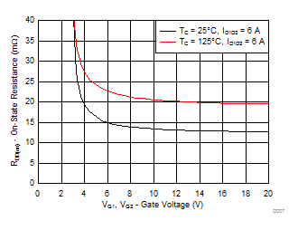
RDD(on) vs VGS

4 Revision History
| DATE | REVISION | NOTES |
|---|---|---|
| September 2017 | * | Initial release. |