SLPS597C April 2017 – April 2018 CSD88599Q5DC
PRODUCTION DATA
- 1Features
- 2Applications
- 3Description
- 4Revision History
- 5Specifications
-
6Application and Implementation
- 6.1 Application Information
- 6.2 Brushless DC Motor With Trapezoidal Control
- 6.3 Power Loss Curves
- 6.4 Safe Operating Area (SOA) Curve
- 6.5 Normalized Power Loss Curves
- 6.6 Design Example – Regulate Current to Maintain Safe Operation
- 6.7 Design Example – Regulate Board and Case Temperature to Maintain Safe Operation
- 7Layout
- 8Device and Documentation Support
- 9Mechanical, Packaging, and Orderable Information
Package Options
Mechanical Data (Package|Pins)
- DMM|22
Thermal pad, mechanical data (Package|Pins)
Orderable Information
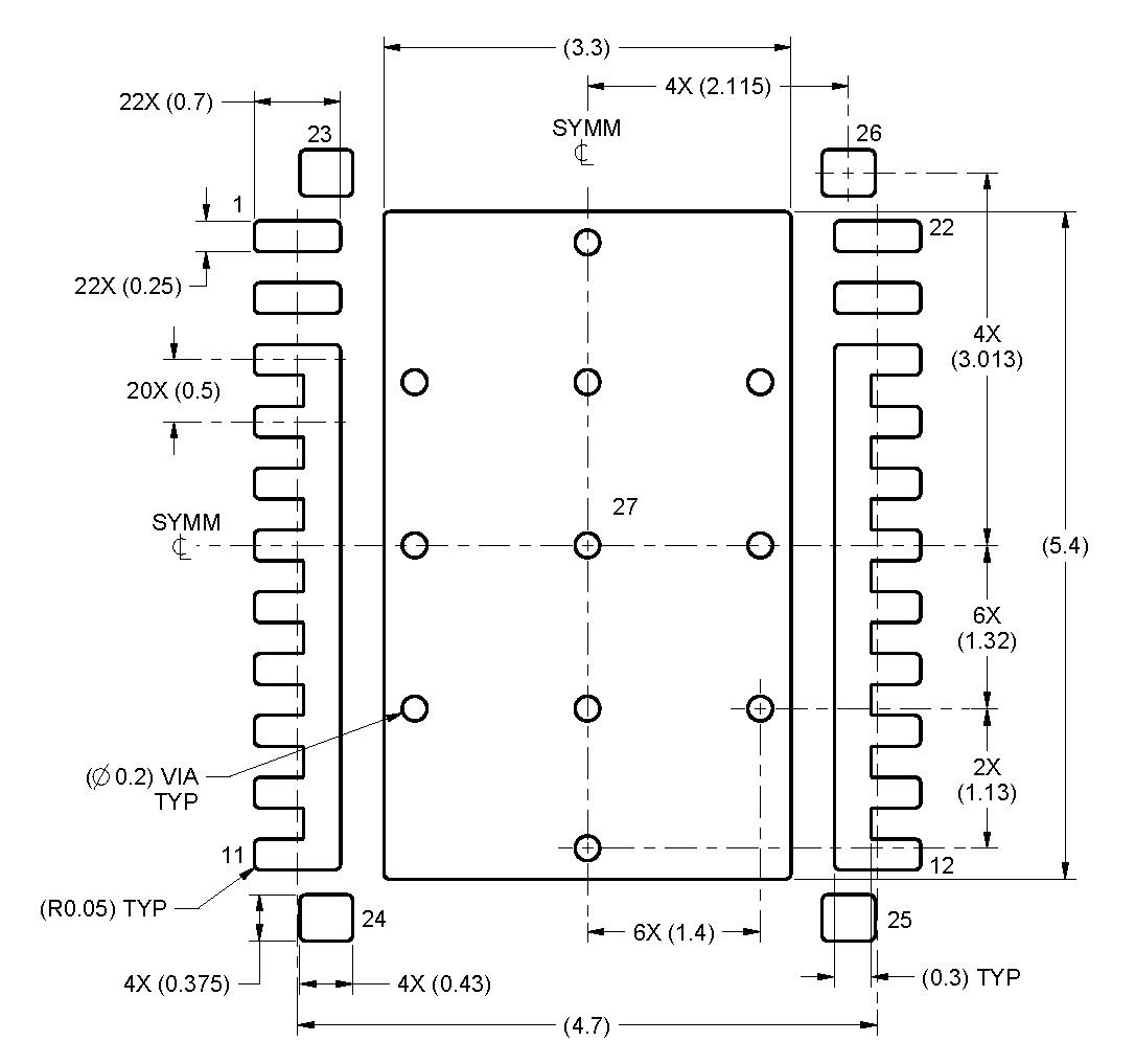
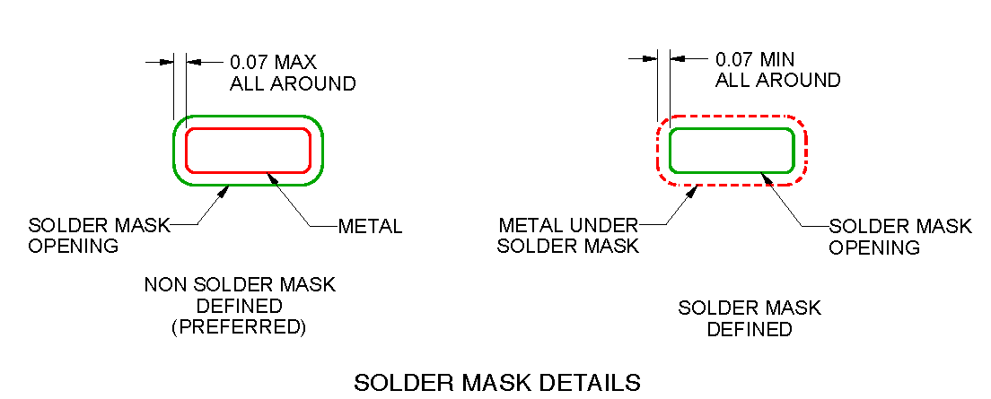
9.2 Land Pattern Recommendation


- All linear dimensions are in millimeters. Any dimensions in parenthesis are for reference only. Dimensioning and tolerancing per ASME Y14.5M.
- This package is designed to be soldered to a thermal pad on the board. For more information, see QFN/SON PCB Attachment (SLUA271).
- Vias are optional depending on application, refer to device data sheet. If some or all are implemented, recommended via locations are shown.