SNAS410F May 2008 – July 2016 DAC121S101QML-SP
PRODUCTION DATA.
- 1 Features
- 2 Applications
- 3 Description
- 4 Revision History
- 5 Pin Configuration and Functions
-
6 Specifications
- 6.1 Absolute Maximum Ratings
- 6.2 ESD Ratings
- 6.3 Recommended Operating Conditions
- 6.4 Thermal Information
- 6.5 DAC121S101QML-SP Electrical Characteristics DC Parameters
- 6.6 DAC121S101QML-SP Electrical Characteristics AC and Timing Characteristics
- 6.7 DAC121S101QML Electrical Characteristics Radiation Electrical Characteristics
- 6.8 DAC121S101QML-SP Electrical Characteristics Operating Life Test Delta Parameters TA at 25°C
- 6.9 Typical Characteristics
- 7 Detailed Description
- 8 Application and Implementation
- 9 Power Supply Recommendations
- 10Layout
- 11Device and Documentation Support
- 12Mechanical, Packaging, and Orderable Information
Package Options
Mechanical Data (Package|Pins)
- NAC|10
- Y|0
Thermal pad, mechanical data (Package|Pins)
Orderable Information
1 Features
-
5962R07726
- Total Ionizing Dose 100 krad(Si)
- Single Event Latch-up Immune
120 MeV-cm2/mg - Single Event Functional Interrupt Immune
120 MeV-cm2/mg (See Radiation Report)
- Ensured Monotonicity
- Low Power Operation
- Rail-to-Rail Voltage Output
- Power-On Reset to Zero Volts Output
- SYNC Interrupt Facility
- Wide Power Supply Range (2.7 V to 5.5 V)
- Small Packages
- Power-Down Feature
- Key Specifications
- Resolution: 12 Bits
- DNL: +0.21, –0.10 LSB (Typical)
- Output Settling Time: 12.5 µs (Typical)
- Zero Code Error: 2.1 mV (Typical)
- Full-Scale Error: −0.04% FS (Typical)
- Power Dissipation
- Normal Mode: 0.52 mW (3.6 V) and 1.19 mW (5.5 V) Typical
- Power-Down Mode: 0.014 µW (3.6 V) and 0.033 µW (5.5 V) Typical
2 Applications
- Satellites
- Altitude and Orbit Control
- Precision Sensors
- Motor Control
- High Temperatures
3 Description
The DAC121S101QML-SP device is a full-featured, general-purpose, 12-bit voltage-output digital-to-analog converter (DAC) that can operate from a single 2.7-V to 5.5-V supply and consumes just
177 µA of current at 3.6 V. The on-chip output amplifier allows rail-to-rail output swing and the three-wire serial interface operates at clock rates up to
20 MHz over the specified supply voltage range and is compatible with standard SPI, QSPI, MICROWIRE, and DSP interfaces.
The supply voltage for the DAC121S101QML-SP serves as its voltage reference, providing the widest possible output dynamic range. A power-on reset circuit ensures that the DAC output powers up to zero volts and remains there until there is a valid write to the device. A power-down feature reduces power consumption to less than a microWatt.
The low power consumption and small packages of the DAC121S101QML-SP make it an excellent choice for use in battery-operated equipment.
Device Information(1)
| PART NUMBER | GRADE | PACKAGE |
|---|---|---|
| DAC121S101WGRQV | 5962R0722601VZA 100 krad | 10-lead ceramic SOIC |
| DAC121S101WGRLV | 5962R0722602VZA 100 krad ELDRS-Free | 10-lead ceramic SOIC |
| DAC121S101-MDR | 5962R0722601V9A 100 krad | Die |
| DAC121S101WGMPR | Pre-Flight Engineering Prototype | 10-lead ceramic SOIC |
| DAC121S101CVAL | Ceramic Evaluation Board | 10-lead ceramic SOIC |
- For all available packages, see the orderable addendum at the end of the data sheet.
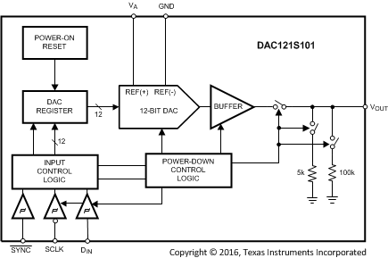
Functional Block Diagram

4 Revision History
Changes from E Revision (March 2013) to F Revision
- Changed data sheet title DAC121S101QML 12-Bit Micro Power Digital-to-Analog Converter With Rail-to-Rail Output to DAC121S101QML-SP Radiation Hardened 12-Bit Micro Power Digital-to-Analog Converter With Rail-to-Rail OutputGo
- Added ESD Ratings table, Feature Description section, Device Functional Modes, Application and Implementation section, Power Supply Recommendations section, Layout section, Device and Documentation Support section, and Mechanical, Packaging, and Orderable Information section.Go
Changes from D Revision (March 2013) to E Revision
- Changed layout of National Data Sheet to TI formatGo