SLAS693C March 2010 – March 2015 DAC3283
PRODUCTION DATA.
- 1 Features
- 2 Applications
- 3 Description
- 4 Simplified Schematic
- 5 Revision History
- 6 Pin Configuration and Functions
-
7 Specifications
- 7.1 Absolute Maximum Ratings
- 7.2 ESD Ratings
- 7.3 Recommended Operating Conditions
- 7.4 Thermal Information
- 7.5 Electrical Characteristics - DC Specifications
- 7.6 Electrical Characteristics - AC Specifications
- 7.7 Electrical Characteristics - Digital Specifications
- 7.8 Timing Requirements
- 7.9 Typical Characteristics
-
8 Detailed Description
- 8.1 Overview
- 8.2 Functional Block Diagram
- 8.3
Feature Description
- 8.3.1
Definition Of Specifications
- 8.3.1.1 Adjacent Carrier Leakage Ratio (ACLR)
- 8.3.1.2 Analog and Digital Power Supply Rejection Ratio (APSSR, DPSSR)
- 8.3.1.3 Differential Nonlinearity (DNL)
- 8.3.1.4 Gain Drift
- 8.3.1.5 Gain Error
- 8.3.1.6 Integral Nonlinearity (INL)
- 8.3.1.7 Intermodulation Distortion (IMD3, IMD)
- 8.3.1.8 Offset Drift
- 8.3.1.9 Offset Error
- 8.3.1.10 Output Compliance Range
- 8.3.1.11 Reference Voltage Drift
- 8.3.1.12 Spurious Free Dynamic Range (SFDR)
- 8.3.1.13 Noise Spectral Density (NSD)
- 8.3.1
Definition Of Specifications
- 8.4
Device Functional Modes
- 8.4.1 Serial Interface
- 8.4.2 Data Interface
- 8.4.3 Input FIFO
- 8.4.4 FIFO Alarms
- 8.4.5 FIFO Modes of Operation
- 8.4.6 Multi-Device Operation
- 8.4.7 Data Pattern Checker
- 8.4.8 DATACLK Monitor
- 8.4.9 FIR Filters
- 8.4.10 Coarse Mixer
- 8.4.11 Quadrature Modulation Correction (QMC)
- 8.4.12 Digital Offset Control
- 8.4.13 Temperature Sensor
- 8.4.14 Sleep Modes
- 8.4.15 LVPECL Inputs
- 8.4.16 LVDS INPUTS
- 8.4.17 CMOS Digital Inputs
- 8.4.18 Reference Operation
- 8.4.19 DAC Transfer Function
- 8.4.20 Analog Current Outputs
- 8.4.21 Passive Interface to Analog Quadrature Modulators
- 8.5
Register Maps
- 8.5.1 CONFIG0 (address = 0x00) [reset = 0x70]
- 8.5.2 CONFIG1 (address = 0x01) [reset = 0x11]
- 8.5.3 CONFIG2 (address = 0x02) [reset = 0x00]
- 8.5.4 CONFIG3 (address = 0x03) [reset = 0x10]
- 8.5.5 CONFIG4 (address = 0x04) [reset = 0xFF]
- 8.5.6 CONFIG5 (address = 0x05) READ ONLY
- 8.5.7 CONFIG6 (address =0x06) [reset = 0x00]
- 8.5.8 CONFIG7 (address = 0x07) [reset = 0x00] (WRITE TO CLEAR)
- 8.5.9 CONFIG8 (address = 0x08) [reset = 0x00] (WRITE TO CLEAR)
- 8.5.10 CONFIG9 (address = 0x09) [reset = 0x7A]
- 8.5.11 CONFIG10 (address = 0x0A) [reset = 0xB6]
- 8.5.12 CONFIG11 (address = 0x0B) [reset = 0xEA]
- 8.5.13 CONFIG12 (address =0x0C) [reset = 0x45]
- 8.5.14 CONFIG13 (address =0x0D) [reset = 0x1A]
- 8.5.15 CONFIG14 Register Name (address = 0x0E) [reset = 0x16]
- 8.5.16 CONFIG15 Register Name (address = 0x0F) [reset = 0xAA]
- 8.5.17 CONFIG16 (address = 0x10) [reset = 0xV6]
- 8.5.18 CONFIG17 (address = 0x11) [reset = 0x24]
- 8.5.19 CONFIG18 (address = 0x12) [reset = 0x02]
- 8.5.20 CONFIG19 (address = 0x13) [reset = 0x00]
- 8.5.21 CONFIG20 (address = 0x14) [reset = 0x00] (CAUSES AUTOSYNC)
- 8.5.22 CONFIG21 (address = 0x15) [reset = 0x00]
- 8.5.23 CONFIG22 (address = 0x16) [reset = 0x00]
- 8.5.24 CONFIG23 (address = 0x17) [reset = 0x00]
- 8.5.25 CONFIG24 (address = 0x18) [reset = 0x83]
- 8.5.26 CONFIG25 (address = 0x19) [reset = 0x00]
- 8.5.27 CONFIG26 (address = 0x1a) [reset = 0x00]
- 8.5.28 CONFIG27 (address =0x1b) [reset = 0x00] (CAUSES AUTOSYNC)
- 8.5.29 CONFIG28 (address = 0x1C) [reset = 0x00]
- 8.5.30 CONFIG29 (address = 0x1D) [reset = 0x00]
- 8.5.31 CONFIG30 (address = 0x1E) [reset = 0x24]
- 8.5.32 VERSION31 (address = 0x1F) [reset = 0x12] (PARTIAL READ ONLY)
- 9 Application and Implementation
- 10Power Supply Recommendations
- 11Layout
- 12Device and Documentation Support
- 13Mechanical, Packaging, and Orderable Information
Package Options
Mechanical Data (Package|Pins)
- RGZ|48
Thermal pad, mechanical data (Package|Pins)
- RGZ|48
Orderable Information
1 Features
- Dual, 16-Bit, 800 MSPS DACs
- 8-Bit Input LVDS Data Bus
- Byte-Wide Interleaved Data Load
- 8 Sample Input FIFO
- Optional Data Pattern Checker
- Multi-DAC Synchronization
- Selectable 2x-4x Interpolation Filters
- Stop-Band Attenuation > 85 dB
- Fs/2 and ± Fs/4 Coarse Mixer
- Digital Quadrature Modulator Correction
- Gain, Phase and Offset Correction
- Temperature Sensor
- 3- or 4-Wire Serial Control Interface
- On-Chip 1.2-V Reference
- Differential Scalable Output: 2 to 20 mA
- Single-Carrier TM1 WCDMA ACLR: 82 dBc at fOUT = 122.88 MHz
- Low Power: 1.3 W at 800 MSPS
- Space Saving Package: 48-pin 7×7mm QFN
2 Applications
- Cellular Base Stations
- Diversity Transmit
- Wideband Communications
- Digital Synthesis
3 Description
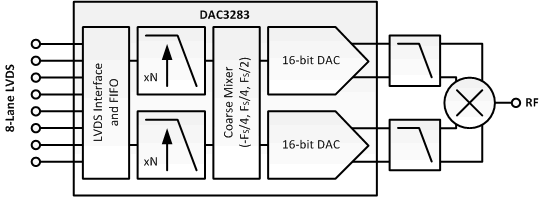
The DAC3283 is a dual-channel 16-bit 800 MSPS digital-to-analog converter (DAC) with an 8-bit LVDS input data bus with on-chip termination, optional 2x-4x interpolation filters, digital IQ compensation and internal voltage reference. The DAC3283 offers superior linearity, noise and crosstalk performance.
Input data can be interpolated by 2x or 4x through on-chip interpolating FIR filters with over 85 dB of stop-band attenuation. Multiple DAC3283 devices can be fully synchronized.
The DAC3283 allows either a complex or real output. An optional coarse mixer in complex mode provides frequency upconversion and the dual DAC output produces a complex Hilbert Transform pair. The digital IQ compensation feature allows optimization of phase, gain and offset to maximize sideband rejection and minimize LO feed-through of an external quadrature modulator performing the final single sideband RF up-conversion.
The DAC3283 is characterized for operation over the entire industrial temperature range of –40°C to 85°C and is available in a 48-pin 7×7mm QFN package.
Device Information(1)
| PART NUMBER | PACKAGE | BODY SIZE (NOM) |
|---|---|---|
| DAC3283 | VQFN (48) | 7.00 mm × 7.00 mm |
- For all available packages, see the orderable addendum at the end of the data sheet.
