SLASE48A November 2014 – January 2015 DAC39J84
PRODUCTION DATA.
- 1 Features
- 2 Applications
- 3 Description
- 4 Revision History
- 5 Pin Configuration and Functions
- 6 Specifications
-
7 Detailed Description
- 7.1 Overview
- 7.2 Functional Block Diagram
- 7.3
Feature Description
- 7.3.1 Serdes Input
- 7.3.2 Serdes Rate
- 7.3.3 Serdes PLL
- 7.3.4 Serdes Equalizer
- 7.3.5 JESD204B Descrambler
- 7.3.6 JESD204B Frame Assembly
- 7.3.7 Serial Peripheral Interface (SPI)
- 7.3.8 Multi-Device Synchronization
- 7.3.9 Input Multiplexer
- 7.3.10 FIR Filters
- 7.3.11 Full Complex Mixer
- 7.3.12 Coarse Mixer
- 7.3.13 Dithering
- 7.3.14 Complex Summation
- 7.3.15 Quadrature Modulation Correction (QMC)
- 7.3.16 Group Delay Correction Block
- 7.3.17 Output Multiplexer
- 7.3.18 Power Measurement And Power Amplifier Protection
- 7.3.19 Serdes Test Modes
- 7.3.20 Error Counter
- 7.3.21 Eye Scan
- 7.3.22 JESD204B Pattern Test
- 7.3.23 Temperature Sensor
- 7.3.24 Alarm Monitoring
- 7.3.25 LVPECL Inputs
- 7.3.26 CMOS Digital Inputs
- 7.3.27 Reference Operation
- 7.3.28 Analog Outputs
- 7.3.29 DAC Transfer Function
- 7.4 Device Functional Modes
- 7.5
Register Map
- 7.5.1
Register Descriptions
- 7.5.1.1 config0 Register - Address: 0x00, Default: 0x0218
- 7.5.1.2 config1 Register - Address: 0x01, Default: 0x0003
- 7.5.1.3 config2 Register - Address: 0x02, Default: 0x2002
- 7.5.1.4 config3 Register - Address: 0x03, Default: 0xF380
- 7.5.1.5 config4 Register - Address: 0x04, Default: 0x00FF
- 7.5.1.6 config5 Register - Address: 0x05, Default: 0xFFFF
- 7.5.1.7 config6 Register - Address: 0x06, Default: 0xFFFF
- 7.5.1.8 config7 Register - Address: 0x07, Default: 0x0000
- 7.5.1.9 config8 Register - Address: 0x08, Default: 0x0000
- 7.5.1.10 config9 Register - Address: 0x09, Default: 0x0000
- 7.5.1.11 config10 Register - Address: 0x0A, Default: 0x0000
- 7.5.1.12 config11 Register - Address: 0x0B, Default: 0x0000
- 7.5.1.13 config12 Register - Address: 0xC, Default: 0x0400
- 7.5.1.14 config13 Register - Address: 0xD, Default: 0x0400
- 7.5.1.15 config14 Register - Address: 0x0E, Default: 0x0400
- 7.5.1.16 config15 Register - Address: 0x0F, Default: 0x0400
- 7.5.1.17 config16 Register - Address: 0x10, Default: 0x0000
- 7.5.1.18 config17 Register - Address: 0x11, Default: 0x0000
- 7.5.1.19 config18 Register - Address: 0x12, Default: 0x0000
- 7.5.1.20 config19 Register - Address: 0x13, Default: 0x0000
- 7.5.1.21 config20 Register - Address: 0x14, Default: 0x0000
- 7.5.1.22 config21 Register - Address: 0x15, Default: 0x0000
- 7.5.1.23 config22 Register - Address: 0x16, Default: 0x0000
- 7.5.1.24 config23 Register - Address: 0x17, Default: 0x0000
- 7.5.1.25 config24 Register - Address: 0x18, Default: 0x0000
- 7.5.1.26 config25 Register - Address: 0x19, Default: 0x0000
- 7.5.1.27 config26 Register - Address: 0x1A, Default: 0x0020
- 7.5.1.28 config27 Register - Address: 0x1B, Default: 0x0000
- 7.5.1.29 config28 Register - Address: 0x1C, Default: 0x0000
- 7.5.1.30 config29 Register - Address: 0x1D, Default: 0x0000
- 7.5.1.31 config30 Register - Address: 0x1E, Default: 0x1111
- 7.5.1.32 config31 Register - Address: 0x1F, Default: 0x1111
- 7.5.1.33 config32 Register - Address: 0x20, Default: 0x0000
- 7.5.1.34 config33 Register - Address: 0x21, Default: 0x0000
- 7.5.1.35 config34 Register - Address: 0x22, Default: 0x1B1B
- 7.5.1.36 config35 Register - Address: 0x23, Default: 0xFFFF
- 7.5.1.37 config36 Register - Address: 0x24, Default: 0x0000
- 7.5.1.38 config37 Register - Address: 0x25, Default: 0x8000
- 7.5.1.39 config38 Register - Address: 0x26, Default: 0x0000
- 7.5.1.40 config39 Register - Address: 0x27, Default: 0x0000
- 7.5.1.41 config40 Register - Address: 0x28, Default: 0x0000
- 7.5.1.42 config41 Register - Address: 0x29, Default: 0x0000
- 7.5.1.43 config42 Register - Address: 0x2A, Default: 0x0000
- 7.5.1.44 config43 Register - Address: 0x2B, Default: 0x0000
- 7.5.1.45 config44 Register - Address: 0x2C, Default: 0x0000
- 7.5.1.46 config45 Register - Address: 0x2D, Default: 0x0000
- 7.5.1.47 config46 Register - Address: 0x2E, Default: 0xFFFF
- 7.5.1.48 config47 Register - Address: 0x2F, Default: 0x0004
- 7.5.1.49 config48 Register - Address: 0x30, Default: 0x0000
- 7.5.1.50 config49 Register - Address: 0x31, Default: 0x0000
- 7.5.1.51 config50 Register - Address: 0x32, Default: 0x0000
- 7.5.1.52 config51 Register - Address: 0x33, Default: 0x0100
- 7.5.1.53 config52 Register - Address: 0x34, Default: 0x0000
- 7.5.1.54 config53 Register - Address: 0x35, Default: 0x0000
- 7.5.1.55 config54 Register - Address: 0x36, Default: 0x0000
- 7.5.1.56 config55 Register - Address: 0x37, Default: 0x0000
- 7.5.1.57 config56 Register - Address: 0x38, Default: 0x0000
- 7.5.1.58 config57 Register - Address: 0x39, Default: 0x0000
- 7.5.1.59 config58 Register - Address: 0x3A, Default: 0x0000
- 7.5.1.60 config59 Register - Address: 0x3B, Default: 0x0000
- 7.5.1.61 config60 Register - Address: 0x3C, Default: 0x0000
- 7.5.1.62 config61 Register - Address: 0x3D, Default: 0x0000
- 7.5.1.63 config62 Register - Address: 0x3E, Default: 0x0000
- 7.5.1.64 config63 Register - Address: 0x3F, Default: 0x0000
- 7.5.1.65 config64 Register - Address: 0x40, Default: 0x0000
- 7.5.1.66 config65 Register - Address: 0x41, Default: 0x0000
- 7.5.1.67 config66 Register - Address: 0x42, Default: 0x0000
- 7.5.1.68 config67 Register - Address: 0x43, Default: 0x0000
- 7.5.1.69 config68 Register - Address: 0x44, Default: 0x0000
- 7.5.1.70 config69 Register - Address: 0x45, Default: 0x0000
- 7.5.1.71 config70 Register - Address: 0x46, Default: 0x0120
- 7.5.1.72 config71 Register - Address: 0x47, Default: 0x3450
- 7.5.1.73 config72 Register - Address: 0x48, Default: 0x31C3
- 7.5.1.74 config73 Register - Address: 0x49, Default: 0x0000
- 7.5.1.75 config74 Register - Address: 0x4A, Default: 0x001E
- 7.5.1.76 config75 Register - Address: 0x4B, Default: 0x0000
- 7.5.1.77 config76 Register - Address: 0x4C, Default: 0x0000
- 7.5.1.78 config77 Register - Address: 0x4D, Default: 0x0300
- 7.5.1.79 config78 Register - Address: 0x4E, Default: 0x0F0F
- 7.5.1.80 config79 Register - Address: 0x4F, Default: 0x1CC1
- 7.5.1.81 config80 Register - Address: 0x50, Default: 0x0000
- 7.5.1.82 config81 Register - Address: 0x51, Default: 0x00FF
- 7.5.1.83 config82 Register - Address: 0x52, Default: 0x00FF
- 7.5.1.84 config83 Register - Address: 0x53, Default: 0x0000
- 7.5.1.85 config84 Register - Address: 0x54, Default: 0x00FF
- 7.5.1.86 config85 Register - Address: 0x55, Default: 0x00FF
- 7.5.1.87 config86 Register - Address: 0x56, Default: 0x0000
- 7.5.1.88 config87 Register - Address: 0x57, Default: 0x00FF
- 7.5.1.89 config88 Register - Address: 0x58, Default: 0x00FF
- 7.5.1.90 config89 Register - Address: 0x59, Default: 0x0000
- 7.5.1.91 config90 Register - Address: 0x5A, Default: 0x00FF
- 7.5.1.92 config91 Register - Address: 0x5B, Default: 0x00FF
- 7.5.1.93 config92 Register - Address: 0x5C, Default: 0x1111
- 7.5.1.94 config93 Register - Address: 0x5D, Default: 0x0000
- 7.5.1.95 config94 Register - Address: 0x5E, Default: 0x0000
- 7.5.1.96 config95 Register - Address: 0x5F, Default: 0x0123
- 7.5.1.97 config96 Register - Address: 0x60, Default: 0x4567
- 7.5.1.98 config97 Register - Address: 0x61, Default: 0x000F
- 7.5.1.99 config98 Register - Address: 0x62, Default: 0x0000
- 7.5.1.100 config99 Register - Address: 0x63, Default: 0x0000
- 7.5.1.101 config100 Register - Address: 0x64, Default: 0x0000
- 7.5.1.102 config101 Register - Address: 0x65, Default: 0x0000
- 7.5.1.103 config102 Register - Address: 0x66, Default: 0x0000
- 7.5.1.104 config103 Register - Address: 0x67, Default: 0x0000
- 7.5.1.105 config104 Register - Address: 0x68, Default: 0x0000
- 7.5.1.106 config105 Register - Address: 0x69, Default: 0x0000
- 7.5.1.107 config106 Register - Address: 0x6A, Default: 0x0000
- 7.5.1.108 config107 Register - Address: 0x6B, Default: 0x0000
- 7.5.1.109 config108 Register - Address: 0x6C, Default: 0x0000
- 7.5.1.110 config109 Register - Address: 0x6D, Default: 0x00xx
- 7.5.1.111 config110 Register - Address: 0x6E, Default: 0x0000
- 7.5.1.112 config111 Register - Address: 0x6F, Default: 0x0000
- 7.5.1.113 config112 Register - Address: 0x70, Default: 0x0000
- 7.5.1.114 config113 Register - Address: 0x71, Default: 0x0000
- 7.5.1.115 config114 Register - Address: 0x72, Default: 0x0000
- 7.5.1.116 config115 Registe - Address: 0x73, Default: 0x0000
- 7.5.1.117 config116 Register - Address: 0x74, Default: 0x0000
- 7.5.1.118 config117 Register - Address: 0x75, Default: 0x0000
- 7.5.1.119 config118 Register - Address: 0x76, Default: 0x0000
- 7.5.1.120 config119 Register - Address: 0x77, Default: 0x0000
- 7.5.1.121 config120 Register - Address: 0x78, Default: 0x0000
- 7.5.1.122 config121 Register - Address: 0x79, Default: 0x0000
- 7.5.1.123 config122 Register - Address: 0x7A, Default: 0x0000
- 7.5.1.124 config123 Register - Address: 0x7B, Default: 0x0000
- 7.5.1.125 config124 Register - Address: 0x7C, Default: 0x0000
- 7.5.1.126 config125 Register - Address: 0x7D, Default: 0x0000
- 7.5.1.127 config126 Register - Address: 0x7E, Default: 0x0000
- 7.5.1.128 config127 Register - Address: 0x7F, Default: 0x0009
- 7.5.1
Register Descriptions
- 8 Applications and Implementation
- 9 Power Supply Recommendations
- 10Layout
- 11Device and Documentation Support
- 12Mechanical, Packaging, and Orderable Information
Package Options
Mechanical Data (Package|Pins)
- AAV|144
Thermal pad, mechanical data (Package|Pins)
Orderable Information
6 Specifications
6.1 Absolute Maximum Ratings
over operating free-air temperature range (unless otherwise noted)(1)| MIN | MAX | UNIT | ||
|---|---|---|---|---|
| Supply Voltage Range(2) | VDDDAC09, VDDDIG09 | –0.3 | 1.3 | V |
| VDDCLK09 | –0.3 | 1.3 | V | |
| VDDT09 | –0.3 | 1.3 | V | |
| VDDR18, VDDIO, VDDS18, VQPS18 | –0.3 | 2.45 | V | |
| VDDAPLL18, VDDAREF18 | –0.3 | 2.45 | V | |
| VDDADAC33 | –0.3 | 4.0 | V | |
| Terminal Voltage Range(2) | RX[7..0]P/N | –0.5 | VDDT09 + 0.5 V | V |
| SDENB, SCLK, SDIO, SDO, TXENA, ALARM, RESETB, SLEEP, TMS, TCLK, TDI, TDO, TRSTB, TESTMODE, SYNC_N_AB, SYNC_N_CD | –0.5 | VDDIO18 + 0.5 V | V | |
| DACCLKP/N, SYSREFP/N | –0.5 | VDDAPLL18 + 0.5 V | V | |
| SYNCBP/N | –0.5 | VDDS18 + 0.5 V | V | |
| LPF | –0.5 | VDDAPLL18 + 0.5 V | V | |
| IOUTAP/N, IOUTBP/N, IOUTCP/N, IOUTDP/N | –0.5 | 1.0 V | V | |
| RBIAS, EXTIO, ATEST | –0.5 | VDDAREF18 + 0.5 V | V | |
| IFORCE, VSENSE | –0.5 | VDDDIG09 + 0.5 V | V | |
| AMUX1, AMUX0 | –0.5 | VDDT09 + 0.5 V | V | |
| Peak input current (any input) | 20 | mA | ||
| Peak total input current (all inputs) | –30 | mA | ||
| Absolute maximum junction temperature TJ | 150 | °C | ||
| Operating free-air temperature, TA: DAC39J84 | –40 | 85 | °C | |
| Storage temperature, Tstg | –65 | 150 | °C | |
(1) Stresses beyond those listed under absolute maximum ratings may cause permanent damage to the device. These are stress ratings only and functional operation of these or any other conditions beyond those indicated under “recommended operating conditions” is not implied. Exposure to absolute-maximum-rated conditions for extended periods may affect device reliability.
(2) Measured with respect to GND.
6.2 ESD Ratings
| VALUE | UNIT | |||
|---|---|---|---|---|
| V(ESD) | Electrostatic discharge | Human body model (HBM), per ANSI/ESDA/JEDEC JS-001(1) | 1000 | V |
| Charged device model (CDM), per JEDEC specification JESD22-C101(2) | 250 | |||
(1) Level listed above is the passing level per ANSI, ESDA, and JEDEC JS-001. JEDEC document JEP155 states that 500-V HBM allows safe manufacturing with a standard ESD control process.
(2) Level listed above is the passing level per EIA-JEDEC JESD22-C101. JEDEC document JEP157 states that 250-V CDM allows safe manufacturing with a standard ESD control process.
6.3 Recommended Operating Conditions
| MIN | NOM | MAX | UNIT | ||
|---|---|---|---|---|---|
| TJ | Recommended operating junction temperature(1) | 105 | °C | ||
| Maximum rated operating junction temperature | 125 | °C | |||
| TA | Recommended free-air temperature | -40 | 25 | 85 | °C |
(1) Prolonged use at this junction temperature may increase the device failure-in-time (FIT) rate.
6.4 Thermal Information
| THERMAL METRICS(1)(2) | DAC39J84 | UNIT | |
|---|---|---|---|
| AAV (144 PINS) | |||
| RθJA | Theta junction-to-ambient (still air) | 31.4 | °C/W |
| RθJB | Theta junction-to-board | 12.6 | |
| RθJC | Theta junction-to-case, top | 1.8 | |
| ψJT | Psi junction-to-top of package | 0.2 | |
| ψJB | Psi junction-to-bottom of package | 12 | |
(1) For more information about traditional and new thermal metrics, see the IC Package Thermal Metrics application report, SPRA953.
(2) Air flow or heat sinking reduces θJA and may be required for sustained operation at 85° and maximum operating conditions.
6.5 DC Electrical Characteristics
Typical values at TA = 25°C, full temperature range is TMIN = -40°C to TMAX = 85°C, nominal supplies, unless otherwise noted.| PARAMETER | TEST CONDITIONS | MIN | TYP | MAX | UNIT | |
|---|---|---|---|---|---|---|
| Resolution | 16 | Bits | ||||
| DC ACCURACY | ||||||
| DNL | Differential nonlinearity | 1 LSB = IOUTFS/216 | ±4 | LSB | ||
| INL | Integral nonlinearity | ±6 | LSB | |||
| ANALOG OUTPUT | ||||||
| Coarse gain linearity | ±0.04 | LSB | ||||
| Offset error | Mid code offset | ±0.001 | %FSR | |||
| Gain error | With external reference | ±2 | %FSR | |||
| With internal reference | ±2 | |||||
| Gain mismatch | With internal reference | ±2 | %FSR | |||
| Full scale output current | 20 | 30 | mA | |||
| Output compliance | –0.5 | 0.6 | V | |||
| Output resistance | 300 | kΩ | ||||
| Output capacitance | 5 | pF | ||||
| REFERENCE OUTPUT | ||||||
| VREF | Reference output voltage | 0.9 | V | |||
| Reference output current(1) | 100 | nA | ||||
| REFERENCE INPUT | ||||||
| VEXTIO | Input voltage | External Reference Mode | 0.1 | 0.9 | 1 | V |
| Input resistance | 1 | MΩ | ||||
| Input capacitance | 50 | pF | ||||
| POWER SUPPLY | ||||||
| VDDADAC33 | 3.15 | 3.3 | 3.45 | V | ||
| VDDAPLL18, VDDAREF18, VDDS18, VQPS18, VDDR18 | 1.71 | 1.8 | 1.89 | V | ||
| VDDIO18 | 1.71 | 1.8 | 1.89 | V | ||
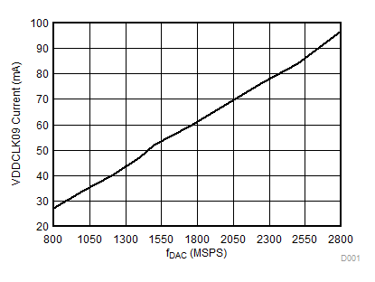
| VDDDIG09, VDDDAC09, VDDCLK09, VDDT09 | fDAC≤2.5GSPS | 0.85 | 0.9 | 1.05 | V | |
| fDAC>2.5GSPS | 0.9 | 1.0 | 1.05 | |||
| POWER CONSUMPTION | ||||||
| I(VDDADAC33) | Analog supply current | MODE 1: fDAC=2.8GSPS, 4x interpolation, NCO on, QMC on, inverse sinc on, GDC off, PAP off, PLL off, LMF=841, SerDes rate = 7Gbps, 20mA FS output, IF=150MHz. |
116 | 130 | mA | |
| I(VDDDIG09) | Digital supply current | 927 | 1150 | |||
| I(VDDDAC09) | DAC supply current | 24 | 30 | |||
| I(VDDCLK09) | Clock supply current | 109 | 140 | |||
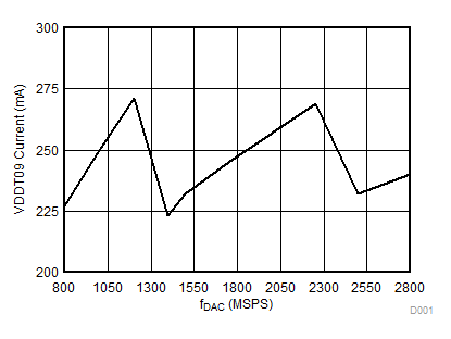
| I(VDDT09) | SerDes core supply current | 266 | 300 | |||
| I(VDDR18) | SerDes analog supply current | 25 | 35 | |||
| I(VDD18) | Other 1.8V supply current | 42 | 65 | |||
| P | Power Dissipation | 1866 | 2190 | mW | ||
| I(VDDADAC33) | Analog supply current | MODE 2: fDAC=2.5GSPS, 2x interpolation, NCO on, QMC on, invsinc on, GDC off, PAP off, PLL on, LMF=841, SerDes rate = 12.5Gbps, 20mA FS output, IF=150MHz. |
114 | mA | ||
| I(VDDDIG09) | Digital supply current | 1026 | ||||
| I(VDDDAC09) | DAC supply current | 20 | ||||
| I(VDDCLK09) | Clock supply current | 87 | ||||
| I(VDDT09) | SerDes core supply current | 323 | ||||
| I(VDDR18) | SerDes analog supply current | 37 | ||||
| I(VDD18) | Other 1.8V supply current | 58 | ||||
| P | Power Dissipation | 1859 | mW | |||
| I(VDDADAC33) | Analog supply current | MODE 3: fDAC=1.47456GSPS, 2x interpolation, NCO on, QMC off, invsinc off, GDC off, PAP off, PLL off, LMF=841, SerDes rate = 7.3728Gbps, 20mA FS output, IF=150MHz. |
114 | mA | ||
| I(VDDDIG09) | Digital supply current | 556 | ||||
| I(VDDDAC09) | DAC supply current | 14 | ||||
| I(VDDCLK09) | Clock supply current | 51 | ||||
| I(VDDT09) | SerDes core supply current | 260 | ||||
| I(VDDR18) | SerDes analog supply current | 24 | ||||
| I(VDD18) | Other 1.8V supply current | 36 | ||||
| P | Power Dissipation | 1277 | mW | |||
| I(VDDADAC33) | Analog supply current | MODE 4: fDAC=1.47456GSPS, 4x interpolation, NCO on, QMC off, invsinc off, GDC off, PAP off, PLL off, LMF=442, SerDes rate = 7.3728Gbps, 20mA FS output, IF=150MHz. |
114 | mA | ||
| I(VDDDIG09) | Digital supply current | 468 | ||||
| I(VDDDAC09) | DAC supply current | 14 | ||||
| I(VDDCLK09) | Clock supply current | 50 | ||||
| I(VDDT09) | SerDes core supply current | 135 | ||||
| I(VDDR18) | SerDes analog supply current | 12 | ||||
| I(VDD18) | Other 1.8V supply current | 36 | ||||
| P | Power Dissipation | 1063 | mW | |||
| I(VDDADAC33) | Analog supply current | MODE 5: fDAC=1.47456GSPS, x4, NCO off, QMC off, invsinc off, GDC off, PAP off, PLL off, LMF=442, SerDes rate = 7.3728Gbps, 20mA FS output, IF=150MHz. |
114 | mA | ||
| I(VDDDIG09) | Digital supply current | 413 | ||||
| I(VDDDAC09) | DAC supply current | 10 | ||||
| I(VDDCLK09) | Clock supply current | 50 | ||||
| I(VDDT09) | SerDes core supply current | 135 | ||||
| I(VDDR18) | SerDes analog supply current | 12 | ||||
| I(VDD18) | Other 1.8V supply current | 28 | ||||
| P | Power Dissipation | 995 | mW | |||
| I(VDDADAC33) | Analog supply current | MODE 6: fDAC=1000MSPS, 2x interpolation, NCO off, QMC off, invsinc off, GDC off, PAP off, PLL on, LMF=442, SerDes rate = 10Gbps, 20mA FS output, IF=150MHz. |
114 | mA | ||
| I(VDDDIG09) | Digital supply current | 373 | ||||
| I(VDDDAC09) | DAC supply current | 12 | ||||
| I(VDDCLK09) | Clock supply current | 37 | ||||
| I(VDDT09) | SerDes core supply current | 151 | ||||
| I(VDDR18) | SerDes analog supply current | 15 | ||||
| I(VDD18) | Other 1.8V supply current | 56 | ||||
| P | Power Dissipation | 1020 | mW | |||
| I(VDDADAC33) | Analog supply current | MODE 7: fDAC=1000MSPS, 2x interpolation, NCO off, QMC off invsinc off, GDC off, PAP off, PLL off, LMF=442, SerDes rate = 10Gbps, 20mA FS output, IF=150MHz. |
114 | mA | ||
| I(VDDDIG09) | Digital supply current | 372 | ||||
| I(VDDDAC09) | DAC supply current | 12 | ||||
| I(VDDCLK09) | Clock supply current | 35 | ||||
| I(VDDT09) | SerDes core supply current | 151 | ||||
| I(VDDR18) | SerDes analog supply current | 15 | ||||
| I(VDD18) | Other 1.8V supply current | 35 | ||||
| P | Power Dissipation | 979 | mW | |||
| I(VDDADAC33) | Analog supply current | MODE 8: fDAC=625MSPS, 2x interpolation, NCO off, QMC off, invsinc off, GDC off, PAP off, PLL off, LMF=841, SerDes rate = 3.125Gbps, 20mA FS output, IF=20MHz. |
114 | mA | ||
| I(VDDDIG09) | Digital supply current | 247 | ||||
| I(VDDDAC09) | DAC supply current | 5 | ||||
| I(VDDCLK09) | Clock supply current | 22 | ||||
| I(VDDT09) | SerDes core supply current | 228 | ||||
| I(VDDR18) | SerDes analog supply current | 21 | ||||
| I(VDD18) | Other 1.8V supply current | 26 | ||||
| P | Power Dissipation | 913 | mW | |||
| I(VDDADAC33) | Analog supply current | MODE 9: fDAC=1.23GSPS, no interpolation, NCO off, QMC off, invsinc off, GDC off, PAP off, PLL off, LMF=841, SerDes rate = 12.3Gbps, 20mA FS output, IF=150MHz; |
114 | mA | ||
| I(VDDDIG09) | Digital supply current | 477 | ||||
| I(VDDDAC09) | DAC supply current | 12 | ||||
| I(VDDCLK09) | Clock supply current | 44 | ||||
| I(VDDT09) | SerDes core supply current | 322 | ||||
| I(VDDR18) | SerDes analog supply current | 39 | ||||
| I(VDD18) | Other 1.8V supply current | 36 | ||||
| P | Power Dissipation | 1261 | mW | |||
| I(VDDADAC33) | Analog supply current | MODE 10: Power down mode, no clock, DAC in sleep mode, SerDes in sleep mode |
5 | mA | ||
| I(VDDDIG09) | Digital supply current | 75 | ||||
| I(VDDDAC09) | DAC supply current | 1 | ||||
| I(VDDCLK09) | Clock supply current | 1 | ||||
| I(VDDT09) | SerDes core supply current | 9 | ||||
| I(VDDR18) | SerDes analog supply current | 0 | ||||
| I(VDD18) | Other 1.8V supply current | 10 | ||||
| P | Power Dissipation | 112 | mW | |||
(1) Use an external buffer amplifier with high impedance input to drive any external load
6.6 Digital Electrical Characteristics
Typical values at TA = 25°C, full temperature range is TMIN = –40°C to TMAX = 85°C, nominal supplies, unless otherwise noted.| PARAMETER | TEST CONDITIONS | MIN | TYP | MAX | UNIT | ||
|---|---|---|---|---|---|---|---|
| CML SERDES INPUTS: RX[7:0]P/N | |||||||
| VDIFF | Receiver Input Amplitude | 50 | 1200 | mV | |||
| VCOM | Input Common Mode (TERM=111) | 600 | mV | ||||
| Input Common Mode (TERM=001) | 700 | ||||||
| Input Common Mode (TERM=100) | 0 | ||||||
| Input Common Mode (TERM=101) | 250 | ||||||
| ZDIFF | Internal differential termination | 85 | 100 | 115 | Ω | ||
| fDATA | Serdes bit rate | 0.78125 | 12.5 | Gbps | |||
| LVPECL INPUTS: SYSREFP/N | |||||||
| VCOM | Input common mode voltage | 0.5 | V | ||||
| VIDPP | Differential input peak-to-peak voltage | 400 | 800 | mV | |||
| ZT | Internal termination | 100 | Ω | ||||
| CL | Input capacitance | 2 | pF | ||||
| LVPECL INPUTS: DACCLKP/N | |||||||
| VCOM | Input common mode voltage | 0.5 | V | ||||
| VIDPP | Differential input peak-to-peak voltage | 400 | 800 | mV | |||
| ZT | Internal termination | 100 | Ω | ||||
| CL | Input capacitance | 2 | pF | ||||
| Duty cycle | 40% | 60% | |||||
| fDACCLK | DACCLKP/N Input Frequency | 2.5 | GHz | ||||
| LVDS OUTPUTS: SYNCBP/N | |||||||
| VCOM | Output common mode voltage | 1.2 | V | ||||
| ZT | Internal termination | 100 | Ω | ||||
| VOD | Differential output voltage swing | 0.5 | V | ||||
| CMOS INTERFACE: SDENB, SCLK, SDIO, SDO, TXENA, ALARM, RESETB, SLEEP, TMS, TCLK, TDI, TDO, TRSTB, TESTMODE, SYNC_N_AB, SYNC_N_CD | |||||||
| VIH | High-level input voltage | 0.7 x VDDIO | V | ||||
| VIL | Low-level input voltage | 0.3 x VDDIO | V | ||||
| IIH | High-level input current | -40 | 40 | µA | |||
| IIL | Low-level input current | -40 | 40 | µA | |||
| CI | CMOS Input capacitance | 2 | pF | ||||
| VOH | ALARM, SDO, SDIO, TDO | Iload =–100 μA | VDDIO – 0.2 | V | |||
| Iload = –2 mA | 0.8 x VDDIO | ||||||
| VOL | ALARM, SDO, SDIO, TDO | Iload = 100 μA | 0.2 | V | |||
| Iload = 2 mA | 0.5 | ||||||
| PHASE LOCKED LOOP(1) | |||||||
| PLL/VCO Operating Frequency | H-Band, pll_vcosel = '0', pll_vcoitune = '11', | pll_vco = '001010'(10) | 4559.9 | 4563.0 | 4566.2 | MHz | |
| pll_vco = '001011'(11) | 4572.7 | 4575.9 | 4579.2 | ||||
| pll_vco = '001100'(12) | 4585.7 | 4589.0 | 4592.3 | ||||
| pll_vco = '001101'(13) | 4599 | 4602.3 | 4608 | ||||
| pll_vco = '001110'(14) | 4612.5 | 4615.9 | 4619.3 | ||||
| pll_vco = '001111'(15) | 4626.2 | 4629.7 | 4633.1 | ||||
| pll_vco = '010000'(16) | 4640.1 | 4643.6 | 4647.2 | ||||
| pll_vco = '010001'(17) | 4654.3 | 4657.8 | 4661.4 | ||||
| pll_vco = '010010'(18) | 4668.6 | 4672.3 | 4675.9 | ||||
| pll_vco = '010011'(19) | 4683.2 | 4686.9 | 4690.6 | ||||
| pll_vco = '010100'(20) | 4698 | 4701.8 | 4705.5 | ||||
| pll_vco = '010101'(21) | 4713.1 | 4716.9 | 4720.7 | ||||
| pll_vco = '010110'(22) | 4728.3 | 4732.2 | 4736 | ||||
| pll_vco = '010111'(23) | 4743.8 | 4747.7 | 4751.6 | ||||
| pll_vco = '011000'(24) | 4759.5 | 4763.4 | 4767.4 | ||||
| pll_vco = '011001'(25) | 4775.4 | 4779.4 | 4783.4 | ||||
| pll_vco = '011010'(26) | 4791.5 | 4795.6 | 4800 | ||||
| pll_vco = '011011'(27) | 4807.9 | 4812.0 | 4816.1 | ||||
| pll_vco = '011100'(28) | 4824.4 | 4828.6 | 4832.8 | ||||
| pll_vco = '011101'(29) | 4841.2 | 4945.4 | 4849.7 | ||||
| pll_vco = '011110'(30) | 4858.2 | 4862.5 | 4866.8 | ||||
| pll_vco = '011111'(31) | 4875.4 | 4879.8 | 4884.1 | ||||
| PLL/VCO Operating Frequency | H-Band, pll_vcosel = '0', pll_vcoitune = '11', | pll_vco = '100000'(32) | 4892.9 | 4897.3 | 4901.7 | MHz | |
| pll_vco = '100001'(33) | 4910.6 | 4915.0 | 4919.5 | ||||
| pll_vco = '100010'(34) | 4928.4 | 4933.0 | 4937.5 | ||||
| pll_vco = '100011'(35) | 4946.6 | 4951.1 | 4955.7 | ||||
| pll_vco = '100100'(36) | 4964.9 | 4969.5 | 4974.1 | ||||
| pll_vco = '100101'(37) | 4983.4 | 4988.1 | 4992.8 | ||||
| pll_vco = '100110'(38) | 5000 | 5006.9 | 5011.7 | ||||
| pll_vco = '100111'(39) | 5021.2 | 5026.0 | 5030.8 | ||||
| pll_vco = '101000'(40) | 5040.4 | 5045.2 | 5050.1 | ||||
| pll_vco = '101001'(41) | 5059.8 | 5064.7 | 5069.6 | ||||
| pll_vco = '101010'(42) | 5079.5 | 5084.4 | 5089.4 | ||||
| pll_vco = '101011'(43) | 5099.3 | 5104.3 | 5109.3 | ||||
| pll_vco = '101100'(44) | 5119.4 | 5124.5 | 5129.5 | ||||
| pll_vco = '101101'(45) | 5139.7 | 5144.8 | 5150 | ||||
| pll_vco = '101110'(46) | 5160.3 | 5165.4 | 5170.6 | ||||
| pll_vco = '101111'(47) | 5180 | 5186.2 | 5191.5 | ||||
| pll_vco = '110000'(48) | 5202 | 5207.2 | 5212.5 | ||||
| pll_vco = '110001'(49) | 5223.2 | 5228.5 | 5233.8 | ||||
| pll_vco = '110010'(50) | 5244.6 | 5250.0 | 5255.3 | ||||
| pll_vco = '110011'(51) | 5266.2 | 5271.6 | 5277.1 | ||||
| pll_vco = '110100'(52) | 5288 | 5293.5 | 5299 | ||||
| pll_vco = '110101'(53) | 5310.1 | 5315.7 | 5321.2 | ||||
| pll_vco = '110110'(54) | 5332.4 | 5338.0 | 5343.6 | ||||
| pll_vco = '110111'(55) | 5354.9 | 5360.6 | 5366.2 | ||||
| pll_vco = '111000'(56) | 5377.6 | 5383.3 | 5389.1 | ||||
| pll_vco = '111001'(57) | 5400.6 | 5406.3 | 5412.1 | ||||
| PLL/VCO Operating Frequency | L-Band, pll_vcosel = '1', pll_vcoitune = '10', | pll_vco = '001010'(10) | 3847.1 | 3849.8 | 3852.4 | MHz | |
| pll_vco = '001011'(11) | 3857.8 | 3860.5 | 3863.2 | ||||
| pll_vco = '001100'(12) | 3868.7 | 3871.4 | 3874.1 | ||||
| pll_vco = '001101'(13) | 3879.7 | 3882.5 | 3885.3 | ||||
| pll_vco = '001110'(14) | 3890.9 | 3893.7 | 3896.6 | ||||
| pll_vco = '001111'(15) | 3902.3 | 3905.2 | 3908 | ||||
| pll_vco = '010000'(16) | 3913.8 | 3916.8 | 3919.7 | ||||
| pll_vco = '010001'(17) | 3925.6 | 3928.6 | 3932.16 | ||||
| pll_vco = '010010'(18) | 3937.5 | 3940.5 | 3943.5 | ||||
| pll_vco = '010011'(19) | 3949.6 | 3952.7 | 3955.7 | ||||
| pll_vco = '010100'(20) | 3961.9 | 3965.0 | 3968.1 | ||||
| pll_vco = '010101'(21) | 3974.7 | 3977.5 | 3980.7 | ||||
| pll_vco = '010110'(22) | 3987 | 3990.2 | 3993.4 | ||||
| pll_vco = '010111'(23) | 3999.8 | 4003.1 | 4006.3 | ||||
| pll_vco = '011000'(24) | 4012.8 | 4016.1 | 4019.4 | ||||
| pll_vco = '011001'(25) | 4026 | 4029.3 | 4032.7 | ||||
| pll_vco = '011010'(26) | 4039.4 | 4042.8 | 4046.1 | ||||
| pll_vco = '011011'(27) | 4052.9 | 4056.3 | 4059.8 | ||||
| pll_vco = '011100'(28) | 4066.6 | 4070.1 | 4073.6 | ||||
| pll_vco = '011101'(29) | 4080.5 | 4084.0 | 4087.6 | ||||
| pll_vco = '011110'(30) | 4094.6 | 4098.2 | 4101.7 | ||||
| pll_vco = '011111'(31) | 4108.9 | 4112.5 | 4120 | ||||
| PLL/VCO Operating Frequency | L-Band, pll_vcosel = '1', pll_vcoitune = '10', | pll_vco = '100000'(32) | 4123.3 | 4127.0 | 4130.6 | MHz | |
| pll_vco = '100001'(33) | 4137.9 | 4141.6 | 4145.3 | ||||
| pll_vco = '100010'(34) | 4152.7 | 4156.5 | 4160.2 | ||||
| pll_vco = '100011'(35) | 4167.7 | 4171.5 | 4175.3 | ||||
| pll_vco = '100100'(36) | 4182.9 | 4186.7 | 4190.5 | ||||
| pll_vco = '100101'(37) | 4198.2 | 4202.1 | 4205.9 | ||||
| pll_vco = '100110'(38) | 4213.7 | 4217.6 | 4221.5 | ||||
| pll_vco = '100111'(39) | 4229.4 | 4233.4 | 4237.3 | ||||
| pll_vco = '101000'(40) | 4245.3 | 4249.3 | 4253.3 | ||||
| pll_vco = '101001'(41) | 4261.3 | 4265.4 | 4269.4 | ||||
| pll_vco = '101010'(42) | 4277.6 | 4281.6 | 4285.7 | ||||
| pll_vco = '101011'(43) | 4294 | 4298.1 | 4302.2 | ||||
| pll_vco = '101100'(44) | 4310.6 | 4314.7 | 4318.9 | ||||
| pll_vco = '101101'(45) | 4327.3 | 4331.6 | 4335.8 | ||||
| pll_vco = '101110'(46) | 4344.3 | 4348.5 | 4352.8 | ||||
| pll_vco = '101111'(47) | 4361.4 | 4365.7 | 4370 | ||||
| pll_vco = '110000'(48) | 4378.7 | 4383.1 | 4387.4 | ||||
| pll_vco = '110001'(49) | 4396.2 | 4400.6 | 4405 | ||||
| pll_vco = '110010'(50) | 4413.9 | 4418.3 | 4423.68 | ||||
| pll_vco = '110011'(51) | 4431.7 | 4436.2 | 4440.7 | ||||
| pll_vco = '110100'(52) | 4449.7 | 4454.3 | 4458.8 | ||||
| pll_vco = '110101'(53) | 4468 | 4472.5 | 4477.1 | ||||
| pll_vco = '110110'(54) | 4486.3 | 4491.0 | 4495.6 | ||||
| pll_vco = '110111'(55) | 4504.9 | 4509.6 | 4514.2 | ||||
| pll_vco = '111000'(56) | 4523.6 | 4528.4 | 4533.1 | ||||
| pll_vco = '111001'(57) | 4542.6 | 4547.3 | 4552.1 | ||||
(1) PLL range not covered in the table can be achieved with the following recommended pll_vco adjustment: if die temperature >55 C°, increase the pll_vco setting by 1; if the die temperature < 15 C°, decrease the pll_vco setting by 1.
6.7 AC Electrical Characteristics
Typical values at TA = 25°C, full temperature range is TMIN = –40°C to TMAX = 85°C, nominal supplies, unless otherwise noted.| PARAMETER | TEST CONDITIONS | MIN | TYP | MAX | UNIT | |
|---|---|---|---|---|---|---|
| ANALOG OUTPUT (1) | ||||||
| fDAC | Maximum DAC rate | 4x or higher interpolation, PLL Off | 2800 | MSPS | ||
| 4x or higher interpolation, PLL On | 2706 | |||||
| 2x interpolation | 2500 | |||||
| 1x interpolation | 1250 | |||||
| AC PERFORMANCE (2) | ||||||
| SFDR | Spurious Free Dynamic (0 to fDAC/2) |
fDAC = 2.8 GSPS, fOUT = 150 MHz, 0 dBFS | 68 | dBc | ||
| fDAC = 2.8 GSPS, fOUT = 300 MHz, 0 dBFS | 66 | |||||
| fDAC = 2.8 GSPS, fOUT = 150 MHz, -12 dBFS | 67 | |||||
| fDAC = 2.8 GSPS, fOUT = 300 MHz, -12 dBFS | 63 | |||||
| fDAC = 2.5 GSPS, fOUT = 20 MHz, 0 dBFS | 79 | |||||
| fDAC = 2.5 GSPS, fOUT = 70 MHz, 0dBFS | 78 | |||||
| fDAC = 2.5 GSPS, fOUT = 150 MHz, 0 dBFS | 72 | |||||
| fDAC = 2.5 GSPS, fOUT = 230 MHz, 0dBFS | 67 | |||||
| fDAC = 2.5 GSPS, fOUT = 20 MHz, -12 dBFS | 79 | |||||
| fDAC = 2.5 GSPS, fOUT = 70 MHz, –12dBFS | 75 | |||||
| fDAC = 2.5 GSPS, fOUT = 150 MHz, -12 dBFS | 70 | |||||
| fDAC = 2.5 GSPS, fOUT = 230 MHz, –12dBFS | 65 | |||||
| fDAC = 1.6 GSPS, fOUT = 20 MHz, 0 dBFS | 81 | |||||
| fDAC = 1.6 GSPS, fOUT = 70 MHz, 0 dBFS | 77 | |||||
| fDAC = 1.6 GSPS, fOUT = 150 MHz, 0 dBFS | 72 | |||||
| fDAC = 1.6 GSPS, fOUT = 230 MHz, 0 dBFS | 68 | |||||
| fDAC = 1.6 GSPS, fOUT = 20 MHz, -12 dBFS | 76 | |||||
| fDAC = 1.6 GSPS, fOUT = 70 MHz, –12 dBFS | 72 | |||||
| fDAC = 1.6 GSPS, fOUT = 150 MHz, -12 dBFS | 67 | |||||
| fDAC = 1.6 GSPS, fOUT = 230 MHz, –12 dBFS | 64 | |||||
| IMD3 | Third-order two-tone intermodulation distortion Each tone at –6dBFS |
fDAC = 2.8 GSPS, fOUT = 150 ± 0.5 MHz | 76 | dBc | ||
| fDAC = 2.8 GSPS, fOUT = 300 ± 0.5 MHz | 68 | |||||
| fDAC = 2.5 GSPS, fOUT = 70 ± 0.5 MHz | 83 | |||||
| fDAC = 2.5 GSPS, fOUT = 150 ± 0.5 MHz | 75 | |||||
| fDAC = 2.5 GSPS, fOUT = 230 ± 0.5 MHz | 70 | |||||
| fDAC = 2.0 GSPS, fOUT = 70 ± 0.5 MHz | 86 | |||||
| fDAC = 2.0 GSPS, fOUT = 150 ± 0.5 MHz | 78 | |||||
| fDAC = 2.0 GSPS, fOUT = 230 ± 0.5 MHz | 73 | |||||
| fDAC = 1.6 GSPS, fOUT = 70 ± 0.5 MHz | 83 | |||||
| fDAC = 1.6 GSPS, fOUT = 150 ± 0.5 MHz | 73 | |||||
| fDAC = 1.6 GSPS, fOUT = 230 ± 0.5 MHz | 66 | |||||
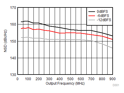
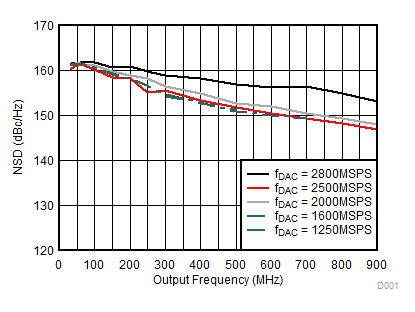
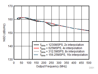
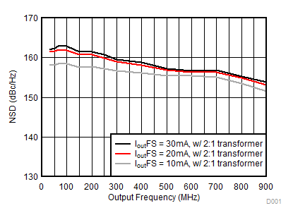
| NSD | Noise Spectral Density(2)
|
fDAC = 2.5 GSPS, fOUT = 70 MHz | -161 | dBFS/Hz | ||
| fDAC = 2.5 GSPS, fOUT = 150 MHz | –159 | |||||
| fDAC = 2.5 GSPS, fOUT = 230 MHz | -157 | |||||
| fDAC = 2.0 GSPS, fOUT = 70 MHz | -161 | |||||
| fDAC = 2.0 GSPS, fOUT = 150 MHz | -160 | |||||
| fDAC = 2.0 GSPS, fOUT = 230 MHz | -158 | |||||
| fDAC = 1.6 GSPS, fOUT = 70 MHz | -161 | |||||
| fDAC = 1.6 GSPS, fOUT = 150 MHz | -159 | |||||
| fDAC = 1.6 GSPS, fOUT = 230 MHz | -157 | |||||
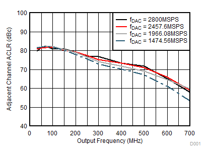
| ACLR(3) | Adjacent channel leakage ratio, single carrier | fDAC = 2.4576 GSPS, fOUT = 70 MHz | 82 | dBc | ||
| fDAC = 2.4576 GSPS, fOUT = 150 MHz | 80 | |||||
| fDAC = 2.4576 GSPS, fOUT = 230 MHz | 78 | |||||
| fDAC = 1.96608 GSPS, fOUT = 70 MHz | 82 | |||||
| fDAC = 1.96608 GSPS, fOUT = 150 MHz | 80 | |||||
| fDAC = 1.96608 GSPS, fOUT = 230 MHz | 77 | |||||
| fDAC = 1.47456 GSPS, fOUT = 70 MHz | 82 | |||||
| fDAC = 1.47456 GSPS, fOUT = 150 MHz | 80 | |||||
| fDAC = 1.47456 GSPS, fOUT = 230 MHz | 76 | |||||
| Channel Isolation | fDAC = 2.5 GSPS, fOUT = 20 MHz | 93 | dBc | |||
| fDAC = 1.6 GSPS, fOUT = 20 MHz | 93 | |||||
(1) Measured single ended into 50 Ω load.
(2) 2:1 transformer output termination, 50 Ω doubly terminated load.
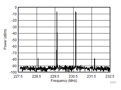
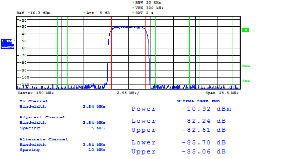
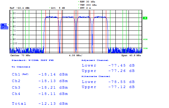
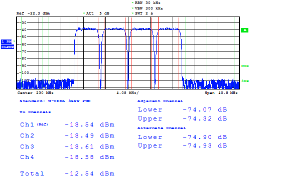
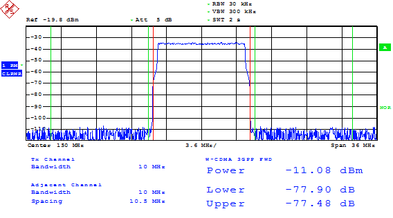
(3) Single carrier, W-CDMA with 3.84 MHz BW, 5-MHz spacing, centered at IF. TESTMODEL 1, 10 ms
6.8 Timing Requirements
Typical values at TA = 25°C, full temperature range is TMIN = –40°C to TMAX = 85°C, nominal supplies, unless otherwise noted.| PARAMETER | TEST CONDITIONS | MIN | TYP | MAX | UNIT | ||
|---|---|---|---|---|---|---|---|
| DIGITAL INPUT TIMING SPECIFICATIONS | |||||||
| TIMING SYSREF INPUT: DACCLKP/N RISING EDGE LATCHING | |||||||
| ts(SYSREF) | Setup time, SYSREFP/N valid to rising edge of DACCLKP/N | 50 | ps | ||||
| th(SYSREF) | Hold time, SYSREF/N valid after rising edge of DACCLKP/N | 50 | ps | ||||
| TIMING SERIAL PORT | |||||||
| ts(SDENB) | Setup time, SDENB to rising edge of SCLK | 20 | ns | ||||
| ts(SDIO) | Setup time, SDIO valid to rising edge of SCLK | 10 | ns | ||||
| th(SDIO) | Hold time, SDIO valid to rising edge of SCLK | 5 | ns | ||||
| t(SCLK) | Period of SCLK | Register config7 read (temperature sensor read) |
1 | µs | |||
| All other registers | 100 | ns | |||||
| td(Data) | Data output delay after falling edge of SCLK | 10 | ns | ||||
| tRESET | Minimum RESETB pulsewidth | 25 | ns | ||||
| ANALOG OUTPUT (1) | |||||||
| ts(DAC) | Output settling time to 0.1% | Transition: Code 0x0000 to 0xFFFF | 10 | ns | |||
| Power-up Time | DAC Wake-up Time | IOUT current settling to 1% of IOUTFS from deep sleep | 90 | µs | |||
| DAC Sleep Time | IOUT current settling to less than 1% of IOUTFS in deep sleep | 90 | |||||
| DELAY/LATENCY | |||||||
| RX SerDes analog delay | 250 | ps | |||||
| RX SerDes digital delay | full rate, RATE = "00" | 34 | UI | ||||
| half rate, RATE = "01" | 29 | ||||||
| quarter rate, RATE = "10" | 26.5 | ||||||
| eighth rate, RATE = "11" | 25.25 | ||||||
| SerDes output to JESD204B elastic buffer input latency | 12-13 | JESD clock cycles | |||||
| SYSREF pin to LMFC reset latency | LMF = 124 and LMF = 244, 2x interpolation | 10 | JESD clock cycles | ||||
| LMF = 124 and LMF = 244, 4x interpolation | 8 | ||||||
| LMF = 124 and LMF = 244, 8x interpolation | 7 | ||||||
| LMF = 124 and LMF = 244, 16x interpolation | 5 | ||||||
| LMF = 222 and LMF = 442, 1x interpolation | 10 | ||||||
| LMF = 222 and LMF = 442, 2x interpolation | 8 | ||||||
| LMF = 222 and LMF = 442, 4x interpolation | 6 | ||||||
| LMF = 222 and LMF = 442, 8x and 16x interpolation | 5 | ||||||
| LMF = 421 and LMF = 841, 1x interpolation | 8 | ||||||
| LMF = 421 and LMF = 841, 2x interpolation | 6 | ||||||
| LMF = 421 and LMF = 841, 4x, 8x and 16x interpolation | 5 | ||||||
| LMF = 821, 1x interpolation | 6 | ||||||
| LMF = 821, 2x, 4x and 8x interpolation | 5 | ||||||
| LMF = 148, 4x interpolation | 11 | ||||||
| LMF = 148, 8x interpolation | 8 | ||||||
| LMF = 148, 16x interpolation | 7 | ||||||
| Digital Latency |
1x interpolation, NCO off, QMC off, Inverse sinc off(2) | 162 | DAC clock cycles | ||||
| 2x Interpolation, NCO off, QMC off, Inverse sinc off(2) | 245 | ||||||
| 4x Interpolation, NCO off, QMC off, Inverse sinc off(2) | 401 | ||||||
| 8x Interpolation, NCO off, QMC off, Inverse sinc off(2) | 740 | ||||||
| 16x Interpolation, NCO off, QMC off, Inverse sinc off(2) | 1423 | ||||||
| NCO | 48 | ||||||
| QMC | 32 | ||||||
| Inverse Sinc | 36 | ||||||
| PA Protection (pap_dlylen_sel = "0") | 68 | ||||||
| Dithering | 0 | ||||||
| Complex Summation | 0 | ||||||
| Coarse Fractional Delay | 51 | ||||||
| Fine Fractional Delay | 52 | ||||||
(1) Measured single ended into 50 Ω load.
(2) Measured latency from JESD buffer release to DAC output, LMF=442.
6.9 Switching Characteristics
Typical values at TA = 25°C, full temperature range is TMIN = –40°C to TMAX = 85°C, nominal supplies, unless otherwise noted.| PARAMETER | TEST CONDITIONS | MIN | TYP | MAX | UNIT | |
|---|---|---|---|---|---|---|
| ANALOG OUTPUT (1) | ||||||
| tpd | Output propagation delay | DAC outputs are updated on the falling edge of DAC clock. Does not include Digital Latency (see below). | 2 | ns | ||
| tr(IOUT) | Output rise time 10% to 90% | 50 | ps | |||
| tf(IOUT) | Output fall time 90% to 10% | 50 | ps | |||
6.10 Typical Characteristics
Unless otherwise noted, all plots are at TA = 25°C, VDDDAC09, VDDCLK09, VDDDIG09 and VDDT09 are at 0.9V, other supplies are at nominal supply voltages, fDAC = 2800MSPS, 4x interpolation, 0dBFS digital input, 20mA full scale output current with 2:1 transformer, LMF = 841 and PLL is disabled.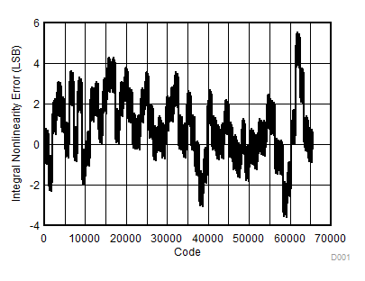 Figure 1. Integral Nonlinearity
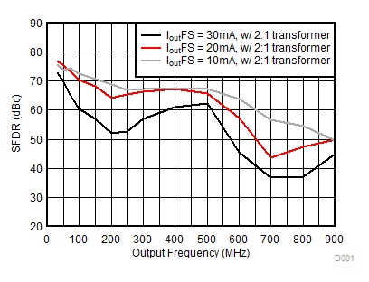
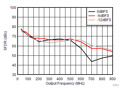 Figure 3. SFDR vs Output Frequency Over Input Scale
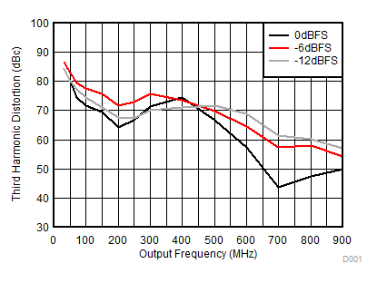 Figure 5. Third Harmonic Distortion vs Output Frequency Over Input Scale
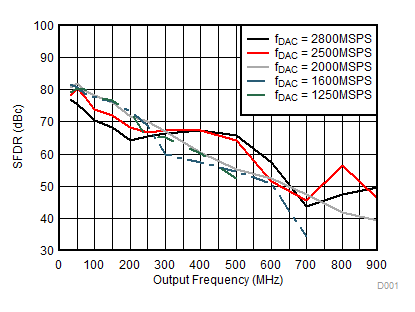
| 4x interpolation for fdac = 2800 msps, 2x interpolation for other cases. |
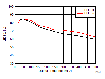
| fref = fDAC/4, M = 32, N = 8, Prescaler = 2 for PLL On, fDAC=2500MSPS, 2x interpolation. |
| IF = 150MHz |
A.
Figure 13. IMD3 vs Output Frequency Over Input Scale
| 4x interpolation for fdac = 2800 msps, 2x interpolation for other cases. |
| fref = fDAC/4, M = 32, N = 8, Prescaler = 2 for PLL On, fDAC=2500MSPS, 2x interpolation. |
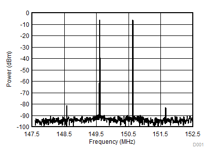
| IF = 150MHz, Tone Spacing = 1MHz |
| 4x interpolation for fdac = 2800 msps, 2x interpolation for other cases. |
| fref = fDAC/4, M = 32, N = 8, Prescaler = 2 for PLL On, fDAC=2500MSPS, 2x interpolation. |
| Single Carrier WCDMA |
| Single Carrier WCDMA; fref = fDAC/4, M = 32, N = 8, Prescaler = 2 for PLL On, fDAC=2500MSPS, 2x interpolation. |
| QMC Off, CMIX Off, NCO Off, LMF=442 for 16x interpolation |
| QMC On, CMIX On, NCO On, LMF=442 for 16x interpolation |
| IF = 70MHz, fDAC=2457.6MSPS | ||
| IF = 230MHz, fDAC=2457.6MSPS | ||
| IF = 150MHz, fDAC=2457.6MSPS | ||
| IF = 70MHz, fDAC=2457.6MSPS | ||
| IF = 230MHz, fDAC=2457.6MSPS | ||
| IF = 150MHz, fDAC=2457.6MSPS | ||
 Figure 2. Differential Nonlinearity
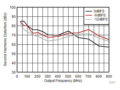 Figure 4. Second Harmonic Distortion vs Output Frequency Over Input Scale
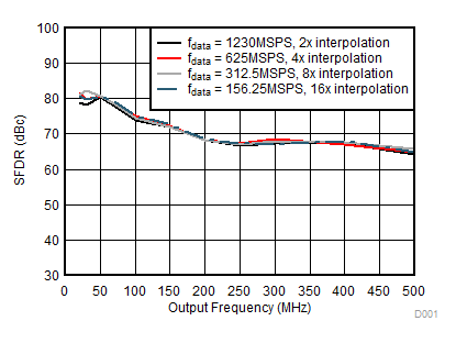 Figure 6. SFDR vs Output Frequency Over Interpolation
| IF = 70MHz |
| IF = 230MHz |
| IF = 70MHz, Tone Spacing = 1MHz |
| IF = 230MHz, Tone Spacing = 1MHz |
| Single Carrier WCDMA |
Single Carrier WCDMA; fref = fDAC/4, M = 32, N = 8, Prescaler = 2 for PLL On, fDAC=2500MSPS, 2x interpolation.
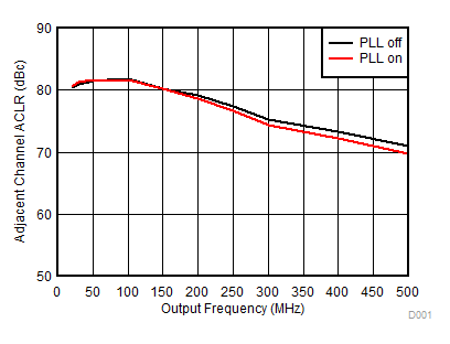
Figure 28. ACLR (Adjacent Channel) vs Output Frequency Over Clocking Options
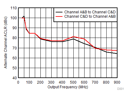
| Between Channel AB pair and CD pair | ||
| QMC Off, CMIX Off, NCO Off, LMF=442 for 16x interpolation |
| QMC On, CMIX On, NCO On, LMF=442 for 16x interpolation |
| IF = 150MHz, fDAC=2457.6MSPS | ||
| IF = 70MHz, fDAC=2457.6MSPS | ||
| IF = 230MHz, fDAC=2457.6MSPS | ||
| IF = 150MHz, fDAC=2457.6MSPS | ||
| IF = 70MHz, fDAC=2457.6MSPS | ||
| IF = 230MHz, fDAC=2457.6MSPS | ||