DLPS048C March 2015 – June 2019 DLPC150
PRODUCTION DATA.
- 1 Features
- 2 Applications
- 3 Description
- 4 Revision History
- 5 Pin Configuration and Functions
-
6 Specifications
- 6.1 Absolute Maximum Ratings
- 6.2 ESD Ratings
- 6.3 Recommended Operating Conditions
- 6.4 Thermal Information
- 6.5 Electrical Characteristics Over Recommended Operating Conditions
- 6.6 Electrical Characteristics
- 6.7 High-Speed Sub-LVDS Electrical Characteristics
- 6.8 Low-Speed SDR Electrical Characteristics
- 6.9 System Oscillators Timing Requirements
- 6.10 Power-Up and Reset Timing Requirements
- 6.11 Parallel Interface Frame Timing Requirements
- 6.12 Parallel Interface General Timing Requirements
- 6.13 Flash Interface Timing Requirements
- 7 Parameter Measurement Information
- 8 Detailed Description
- 9 Application and Implementation
- 10Power Supply Recommendations
-
11Layout
- 11.1
Layout Guidelines
- 11.1.1 PCB Layout Guidelines For Internal Controller PLL Power
- 11.1.2 DLPC150 Reference Clock
- 11.1.3 General PCB Recommendations
- 11.1.4 General Handling Guidelines for Unused CMOS-Type Pins
- 11.1.5 Maximum Pin-to-Pin, PCB Interconnects Etch Lengths
- 11.1.6 Number of Layer Changes
- 11.1.7 Stubs
- 11.1.8 Terminations
- 11.1.9 Routing Vias
- 11.2 Layout Example
- 11.3 Thermal Considerations
- 11.1
Layout Guidelines
- 12Device and Documentation Support
- 13Mechanical, Packaging, and Orderable Information
Package Options
Mechanical Data (Package|Pins)
- ZEZ|201
Thermal pad, mechanical data (Package|Pins)
6.13 Flash Interface Timing Requirements
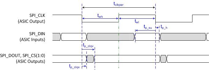
The DLPC150 controller flash memory interface consists of a SPI flash serial interface with a programmable clock rate. The DLPC150 controller can support 1- to 16-Mb flash memories. (see (2)(3))| MIN | MAX | UNIT | |||
|---|---|---|---|---|---|
| ƒclock | Clock frequency, SPI_CLK | See (1) | 1.42 | 36 | MHz |
| tp_clkper | Clock period, SPI_CLK | 50% reference points | 704 | 27.7 | ns |
| tp_wh | Pulse duration low, SPI_CLK | 50% reference points | 352 | ns | |
| tp_wl | Pulse duration high, SPI_CLK | 50% reference points | 352 | ns | |
| tt | Transition time – all signals | 20% to 80% reference points | 0.2 | 3 | ns |
| tp_su | Setup time – SPI_DIN valid before SPI_CLK falling edge | 50% reference points | 10 | ns | |
| tp_h | Hold time – SPI_DIN valid after SPI_CLK falling edge | 50% reference points | 0 | ns | |
| tp_clqv | SPI_CLK clock falling edge to output valid time – SPI_DOUT and SPI_CSZ | 50% reference points | 1 | ns | |
| tp_clqx | SPI_CLK clock falling edge output hold time – SPI_DOUT and SPI_CSZ | 50% reference points | –3 | 3 | ns |
(1) This range include the 200 ppm of the external oscillator (but no jitter).
(2) Standard SPI protocol is to transmit data on the falling edge of SPI_CLK and capture data on the rising edge. The DLPC150 controller does transmit data on the falling edge, but it also captures data on the falling edge rather than the rising edge. This provides support for SPI devices with long clock-to-Q timing. DLPC150 controller hold capture timing has been set to facilitate reliable operation with standard external SPI protocol devices.
(3) With the above output timing, the DLPC150 controller provides the external SPI device 8.2-ns input set-up and 8.2-ns input hold, relative to the rising edge of SPI_CLK.
 Figure 7. Flash Interface Timing