DLPS048C March 2015 – June 2019 DLPC150
PRODUCTION DATA.
- 1 Features
- 2 Applications
- 3 Description
- 4 Revision History
- 5 Pin Configuration and Functions
-
6 Specifications
- 6.1 Absolute Maximum Ratings
- 6.2 ESD Ratings
- 6.3 Recommended Operating Conditions
- 6.4 Thermal Information
- 6.5 Electrical Characteristics Over Recommended Operating Conditions
- 6.6 Electrical Characteristics
- 6.7 High-Speed Sub-LVDS Electrical Characteristics
- 6.8 Low-Speed SDR Electrical Characteristics
- 6.9 System Oscillators Timing Requirements
- 6.10 Power-Up and Reset Timing Requirements
- 6.11 Parallel Interface Frame Timing Requirements
- 6.12 Parallel Interface General Timing Requirements
- 6.13 Flash Interface Timing Requirements
- 7 Parameter Measurement Information
- 8 Detailed Description
- 9 Application and Implementation
- 10Power Supply Recommendations
-
11Layout
- 11.1
Layout Guidelines
- 11.1.1 PCB Layout Guidelines For Internal Controller PLL Power
- 11.1.2 DLPC150 Reference Clock
- 11.1.3 General PCB Recommendations
- 11.1.4 General Handling Guidelines for Unused CMOS-Type Pins
- 11.1.5 Maximum Pin-to-Pin, PCB Interconnects Etch Lengths
- 11.1.6 Number of Layer Changes
- 11.1.7 Stubs
- 11.1.8 Terminations
- 11.1.9 Routing Vias
- 11.2 Layout Example
- 11.3 Thermal Considerations
- 11.1
Layout Guidelines
- 12Device and Documentation Support
- 13Mechanical, Packaging, and Orderable Information
Package Options
Mechanical Data (Package|Pins)
- ZEZ|201
Thermal pad, mechanical data (Package|Pins)
10.1 System Power-Up and Power-Down Sequence
Although the DLPC150 requires an array of power supply voltages, (for example, VDD, VDDLP12, VDD_PLLM/D, VCC18, VCC_FLSH, VCC_INTF), if VDDLP12 is tied to the 1.1-V VDD supply (which is assumed to be the typical configuration), then there are no restrictions regarding the relative order of power supply sequencing to avoid damaging the DLPC150. This is true for both power-up and power-down scenarios. Similarly, there is no minimum time between powering-up or powering-down the different supplies if VDDLP12 is tied to the 1.1-V VDD supply.
If however VDDLP12 is not tied to the VDD supply, then VDDLP12 must be powered-on after the VDD supply is powered-on, and powered-off before the VDD supply is powered-off. In addition, if VDDLP12 is not tied to VDD, then VDDLP12 and VDD supplies must be powered on or powered off within 100 ms of each other.
Although there is no risk of damaging the DLPC150 if the above power sequencing rules are followed, the following additional power sequencing recommendations must be considered to ensure proper system operation.
- To ensure that DLPC150 output signal states behave as expected, all DLPC150 I/O supplies must remain applied while VDD core power is applied. If VDD core power is removed while the I/O supply (VCC_INTF) is applied, then the output signal state associated with the inactive I/O supply will go to a high impedance state.
- Additional power sequencing rules may exist for devices that share the supplies with the DLPC150, and thus these devices may force additional system power sequencing requirements.
Note that when VDD core power is applied, but I/O power is not applied, additional leakage current may be drawn. This added leakage does not affect normal DLPC150 operation or reliability.
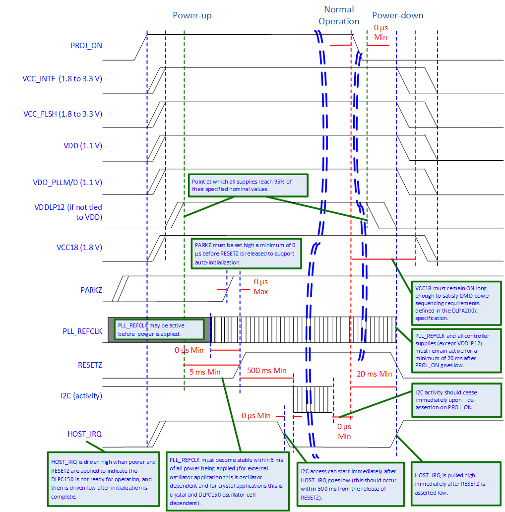
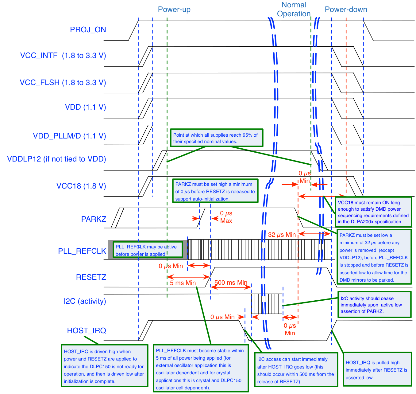
Figure 15 and Figure 16 show the DLPC150 power-up and power-down sequence for both the normal PARK and fast PARK operations of the DLPC150 controller.
 Figure 15. DLPC150 Power-Up / Proj_on = 0 Initiated Normal Park and Power-Down
  Figure 16. DLPC150 Power-Up / PARKZ = 0 Initiated Fast Park and Power-Down