DLPS029F April 2013 – May 2019 DLPC350
PRODUCTION DATA.
- 1 Features
- 2 Applications
- 3 Description
- 4 Revision History
- 5 Pin Configuration and Functions
-
6 Specifications
- 6.1 Absolute Maximum Ratings
- 6.2 ESD Ratings
- 6.3 Recommended Operating Conditions
- 6.4 Thermal Information
- 6.5 I/O Electrical Characteristics
- 6.6 I2C0 and I2C1 Interface Timing Requirements
- 6.7 Port 1 Input Pixel Interface Timing Requirements
- 6.8 Port 2 Input Pixel Interface (FPD-Link Compatible LVDS Input) Timing Requirements
- 6.9 System Oscillator Timing Requirements
- 6.10 Reset Timing Requirements
- 6.11 Video Timing Input Blanking Specification
- 6.12 Programmable Output Clocks Switching Characteristics
- 6.13 DMD Interface Switching Characteristics
- 6.14 JTAG Interface: I/O Boundary Scan Application Switching Characteristics
- 7 Parameter Measurement Information
- 8 Detailed Description
- 9 Application and Implementation
- 10Power Supply Recommendations
-
11Layout
- 11.1 Layout Guidelines
- 11.2 Layout Example
- 12Device and Documentation Support
- 13Mechanical, Packaging, and Orderable Information
Package Options
Mechanical Data (Package|Pins)
- ZFF|419
Thermal pad, mechanical data (Package|Pins)
8.1 Overview
In DLP-based solutions, image data is 100% digital from the DLPC350 input port to the image on the DMD. The image stays in digital form and is not converted into an analog signal. The DLPC350 controller processes the digital input image and converts the data into a format needed by the DMD. The DMD steers light by using binary pulse width modulation (PWM) for each micromirror. For further details, refer to DMD data sheet (TI literature number DLPS028 for the DLP4500 and DLPS032 for the DLP4500NIR).
Figure 13 is the DLPC350 controller functional block diagram. As part of the pixel processing functions, the DLPC350 controller offers format conversion functions: chroma interpolation and color-space conversion. The DLPC350 controller also offers several image-enhancement functions. The DLPC350 controller also supports the necessary functions to format the input data to the DMD. The pixel processing functions allow the DLPC350 controller and DMD to support a wide variety of resolutions including NTSC, PAL, XGA, and WXGA. The pixel processing functions can be optionally bypassed with the native 912 × 1140 pixel resolution to support direct one-to-one pixel mapping.
When accurate pattern display is needed, the native 912 × 1140 input resolution pattern has a one-to-one association with the corresponding micromirror on the DMD. The DLPC350 controller enables high-speed display of these patterns. This functionality is well-suited for techniques such as structured light, additive manufacturing, or digital exposure.
Commands can be input to the DLPC350 controller over an I2C interface.
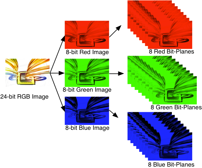
The DLPC350 controller takes as input 24-, 27-, or 30-bit RGB data at up to 120-Hz frame rate. This frame rate is composed of three colors (red, green, and blue) with each color equally divided in the 120-Hz frame rate. Thus, each color has a 2.78-ms time slot allocated. Because each color has an 8-, 9-, or 10-bit depth, each color time slot is further divided into bit-planes. A bit-plane is the 2-dimensional arrangement of one-bit extracted from all the pixels in the full color 2D image to implement dynamic depth (see Figure 11).
 Figure 11. Bit Slices
 The length of each bit-plane in the time slot is weighted by the corresponding power of two of its binary representation. This provides a binary pulse width modulation of the image. For example, a 24-bit RGB input has three colors with 8-bit depth each. Each color time slot is divided into eight bit-planes, with the sum of the weight of all bit planes in the time slot equal to 256. See Figure 12 for an illustration of this partition of the bits in a frame.
 Figure 12. Bit Partition in a Frame for an 8-Bit Color
 Therefore, a single video frame is composed of a series of bit-planes. Because the DMD mirrors can be either on or off, an image is created by turning on the mirrors corresponding to the bit set in a bit-plane. With binary pulse width modulation, the intensity level of the color is reproduced by controlling the amount of time the mirror is on. For a 24-bit RGB frame image input to the DLPC350 controller, the DLPC350 controller creates 24 bit-planes, stores them in a double-buffered eDRAM embedded in the chip, and sends them to the DMD, one bit-plane at a time. Depending on the bit weight of the bit-plane, the DLPC350 controller controls the time this bit-plane is illuminated, controlling the intensity of the bit-plane. To improve image quality in video frames, these bit-planes, time slots, and color frames are shuffled and interleaved with spatial-temporal algorithms by the DLPC350 controller.