DLPS074 February 2017 DLPC4422
PRODUCTION DATA.
- 1 Features
- 2 Applications
- 3 Description
- 4 Revision History
- 5 Pin Configuration and Functions
-
6 Specifications
- 6.1 Absolute Maximum Ratings
- 6.2 ESD Ratings
- 6.3 Recommended Operating Conditions
- 6.4 Thermal Information
- 6.5 Electrical Characteristics
- 6.6 System Oscillators Timing Requirements
- 6.7 Test and Reset Timing Requirements
- 6.8 JTAG Interface: I/O Boundary Scan Application Timing Requirements
- 6.9 Port 1 Input Pixel Timing Requirements
- 6.10 Port 3 Input Pixel Interface (via GPIO) Timing Requirements
- 6.11 DMD LVDS Interface Timing Requirements
- 6.12 Synchronous Serial Port (SSP) Interface Timing Requirements
- 6.13 Programmable Output Clocks Switching Characteristics
- 6.14 Synchronous Serial Port Interface (SSP) Switching Characteristics
- 6.15 JTAG Interface: I/O Boundary Scan Application Switching Characteristics
-
7 Detailed Description
- 7.1 Overview
- 7.2 Functional Block Diagram
- 7.3 Feature Description
- 8 Application and Implementation
- 9 Power Supply Recommendations
- 10Layout
- 11Device and Documentation Support
- 12Mechanical, Packaging, and Orderable Information
Package Options
Mechanical Data (Package|Pins)
- ZPC|516
Thermal pad, mechanical data (Package|Pins)
Orderable Information
1 Features
- Provides Two 30-bit Input Pixel Interfaces or One 60-bit Input Pixel Interface:
- YUV, YCrCb, or RGB Data Format
- 8, 9 or 10 Bits per Color
- Pixel Clock Support Up to 175 MHz for 30-bit and 160 MHz for 60-bit
- Supports 24-30 Hz and 47-120 Hz Frame Rates
- Full Single DLP Controller Support For DMD™s Up to 1920 Pixels Wide
- Dual DLP Controller Support For Up to 4K Ultra High Definition (UHD) Resolution Display Using DLP660TE TRP DMD
- High-Speed, Low Voltage Differential Signaling (LVDS) DMD Interface
- 150 MHz ARM946™ Microprocessor
- Microprocessor Peripherals
- Programmable Pulse-Width Modulation (PWM) and Capture Timers
- Three I2C Ports, Three UART Ports and Three SSP Ports
- One USB 1.1 Slave Port
- Image Processing
- Multiple Image Processing Algorithms
- Frame Rate Conversion
- Color Coordinate Adjustment
- Programmable Color Space Conversion
- Programmable Degamma and Splash
- Integrated Support for 3-D Display
- On-Screen Display (OSD)
- Integrated Clock Generation Circuitry
- Operates on a Single 20 MHz Crystal
- Integrated Spread Spectrum Clocking
- External Memory Support
- Parallel Flash for Microprocessor and PWM Sequence
- Optional SRAM
- 516 Pin Plastic Ball Grid Array Package
- Supports Lamp, LED, and Laser Hybrid Illumination Systems
2 Applications
- 4K Ultra High Definition (UHD) Display
- Laser TV
- Digital Signage
- Projection Mapping
3 Description
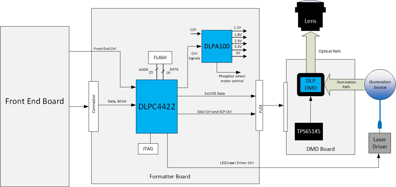
DLPC4422 is a digital display controller for the DLP 4K UHD display chipset. The DLPC4422 display controller, together with the DLP660TE DMD and DLPA100 power management and motor driver device, comprise the chipset. This solution is a great fit for display systems that require high resolution, high brightness and system simplicity. To ensure reliable operation, the DLPC4422 display controller must always be used with the DLP660TE DMD and the DLPA100 power management and motor driver device.
Device Information(1)
| PART NUMBER | PACKAGE | BODY SIZE (NOM) |
|---|---|---|
| DLPC4422 | ZPC (516) | 27.00 mm × 27.00 mm |
- For all available packages, see the orderable addendum at the end of the data sheet.
Simplified Schematic
