DLPS074 February 2017 DLPC4422
PRODUCTION DATA.
- 1 Features
- 2 Applications
- 3 Description
- 4 Revision History
- 5 Pin Configuration and Functions
-
6 Specifications
- 6.1 Absolute Maximum Ratings
- 6.2 ESD Ratings
- 6.3 Recommended Operating Conditions
- 6.4 Thermal Information
- 6.5 Electrical Characteristics
- 6.6 System Oscillators Timing Requirements
- 6.7 Test and Reset Timing Requirements
- 6.8 JTAG Interface: I/O Boundary Scan Application Timing Requirements
- 6.9 Port 1 Input Pixel Timing Requirements
- 6.10 Port 3 Input Pixel Interface (via GPIO) Timing Requirements
- 6.11 DMD LVDS Interface Timing Requirements
- 6.12 Synchronous Serial Port (SSP) Interface Timing Requirements
- 6.13 Programmable Output Clocks Switching Characteristics
- 6.14 Synchronous Serial Port Interface (SSP) Switching Characteristics
- 6.15 JTAG Interface: I/O Boundary Scan Application Switching Characteristics
-
7 Detailed Description
- 7.1 Overview
- 7.2 Functional Block Diagram
- 7.3 Feature Description
- 8 Application and Implementation
- 9 Power Supply Recommendations
- 10Layout
- 11Device and Documentation Support
- 12Mechanical, Packaging, and Orderable Information
Package Options
Mechanical Data (Package|Pins)
- ZPC|516
Thermal pad, mechanical data (Package|Pins)
Orderable Information
8 Application and Implementation
NOTE
Information in the following applications sections is not part of the TI component specification, and TI does not warrant its accuracy or completeness. TI’s customers are responsible for determining suitability of components for their purposes. Customers should validate and test their design implementation to confirm system functionality.
8.1 Application Information
The DLPC4422 display controller is part of the DLP660TE chipset. The controller integrates all system image processing and control and DMD data formatting onto a single integrated circuit (IC). It will support LED, Lamp, or Hybrid illumination systems, and it also includes multiple image processing algorithms such as DynamicBlack™ or BrilliantColor™. Applications of interest include 4K UHD display applications, Laser TV, digital signage and projection mapping.
8.2 Typical Application
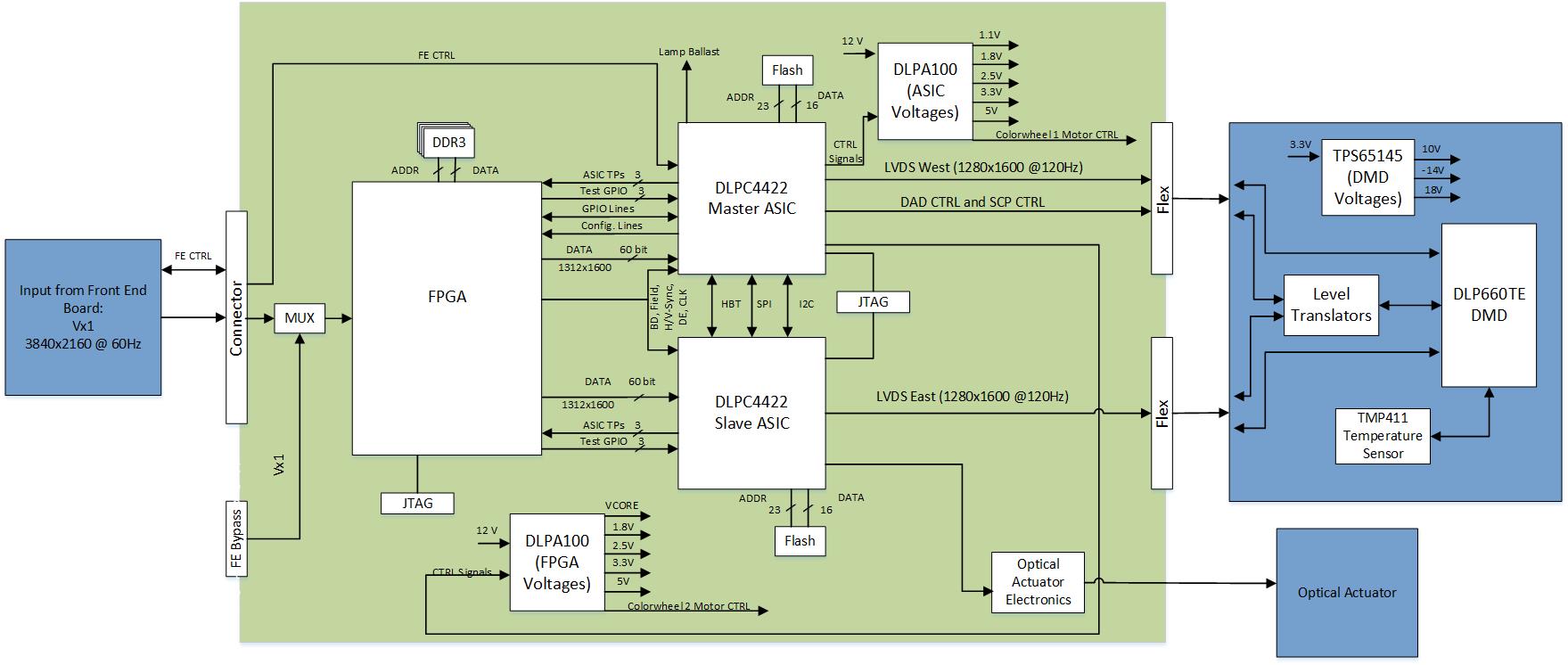
The DLPC4422 controller is ideal for applications requiring high brightness and high resolution displays. When two DLPC4422 display controllers are combined with the DLP660TE DMD, an FPGA, a power management and motor driver device (DLPA100), and other electrical, optical and mechanical components the chipset enables bright, affordable, full 4K UHD display solutions. A typical 4K UHD system application using the DLPC4422 controller and DLP660TE DMD is shown in Figure 10.
 Figure 10. Typical 4K UHD Display Application
8.2.1 Design Requirements
The display controller is the digital interface between the DMD and the rest of the system. The display controller takes digital input from front end digital receivers and drives the DMD over a high speed interface. The display controller also generates the necessary signals (data, protocols, timings) required to display images on the DMD. Some systems require a dual controller to format the incoming data before sending it to the DMD. Reliable operation of the DMD is only insured when the DMD and the controller are used together in a system. In addition to the DLP devices in the chipset, other devices may be needed. Typically a Flash part is needed to store the software and firmware.
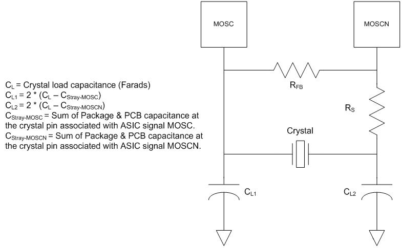
8.2.1.1 Recommended MOSC Crystal Oscillator Configuration
Table 8. Crystal Port Characteristics
| PARAMETER | NOMINAL | UNIT |
|---|---|---|
| MOSC TO GROUND Capacitance | 1.5 | pF |
| MOSCZ TO GROUND Capacitance | 1.5 | pF |
Table 9. Recommended Crystal Configuration
| PARAMETER | RECOMMENDED | UNIT |
|---|---|---|
| Crystal circuit configuration | Parallel resonant | |
| Crystal type | Fundamental (1st Harmonic) | |
| Crystal nominal frequency | 20 | MHz |
| Crystal frequency temperature stability | +/- 30 | PPM |
| Overall crystal frequency tolerance (including accuracy, stability, aging, and trim sensitivity) | +/- 100 | PPM |
| Crystal Equivalent Series Resistor (ESR) | 50 max | Ω |
| Crystal load | 20 | pF |
| Crystal shunt load | 7 max | pF |
| RS drive resistor (nominal) | 100 | Ω |
| RFB feedback resistor (nominal) | 1 | MΩ |
| CL1 external crystal load capacitor (MOSC) | See (1) | pF |
| CL2 external crystal load capacitor (MOSCN) | See (1) | pF |
| PCB layout | TI recommends a ground isolation ring around the crystal. |
 Figure 11. Recommended Crystal Oscillator Configuration
It is assumed that the external crystal oscillator will stabilize within 50 ms after stable power is applied.
8.2.2 Detailed Design Procedure
For connecting the DLPC4422 controller and the DLP660TE DMD together, see the reference design schematic. Layout guidelines should be followed to achieve a reliable projector. To complete the DLP system, an optical module or light engine is required that contains the DLP660TE DMD, associated illumination sources, optical elements, and necessary mechanical components.