DLPS074 February 2017 DLPC4422
PRODUCTION DATA.
- 1 Features
- 2 Applications
- 3 Description
- 4 Revision History
- 5 Pin Configuration and Functions
-
6 Specifications
- 6.1 Absolute Maximum Ratings
- 6.2 ESD Ratings
- 6.3 Recommended Operating Conditions
- 6.4 Thermal Information
- 6.5 Electrical Characteristics
- 6.6 System Oscillators Timing Requirements
- 6.7 Test and Reset Timing Requirements
- 6.8 JTAG Interface: I/O Boundary Scan Application Timing Requirements
- 6.9 Port 1 Input Pixel Timing Requirements
- 6.10 Port 3 Input Pixel Interface (via GPIO) Timing Requirements
- 6.11 DMD LVDS Interface Timing Requirements
- 6.12 Synchronous Serial Port (SSP) Interface Timing Requirements
- 6.13 Programmable Output Clocks Switching Characteristics
- 6.14 Synchronous Serial Port Interface (SSP) Switching Characteristics
- 6.15 JTAG Interface: I/O Boundary Scan Application Switching Characteristics
-
7 Detailed Description
- 7.1 Overview
- 7.2 Functional Block Diagram
- 7.3 Feature Description
- 8 Application and Implementation
- 9 Power Supply Recommendations
- 10Layout
- 11Device and Documentation Support
- 12Mechanical, Packaging, and Orderable Information
Package Options
Mechanical Data (Package|Pins)
- ZPC|516
Thermal pad, mechanical data (Package|Pins)
Orderable Information
6 Specifications
6.1 Absolute Maximum Ratings
over operating free-air temperature range (unless otherwise noted)(1)| MIN | MAX | UNIT | ||
| ELECTRICAL | ||||
| Supply Voltage(2) | VDD11 (Core) | –0.30 | 1.60 | V |
| VDD18 (LVDS I/O and Internal DRAM) | –0.30 | 2.50 | ||
| VDD33 (I/O) | –0.30 | 3.90 | ||
| VDD_PLLD (1.1V DMD clock generator - Digital) | -0.30 | 1.60 | ||
| VDD_PLLM1 (1.1V Master - LS clock generator - Digital) | -0.30 | 1.60 | ||
| VDD_PLLM2 (1.1V Master - HS clock generator - Digital) | -0.30 | 1.60 | ||
| VDD_PLLD (1.8V DMD clock generator - Analog) | -0.30 | 2.50 | ||
| VDD_PLLM1 (1.8V Master - LS clock generator - Analog) | -0.30 | 2.50 | ||
| VDD_PLLM2 (1.8V Master - HS clock generator - Analog) | -0.30 | 2.50 | ||
| VDD_PLLS (1.1V Video 2X - Analog) | -0.50 | 1.40 | ||
| VI Input Voltage(3) | USB | -1.0 | 5.25 | V |
| OSC | -0.3 | VDD33 + 0.3 | ||
| 3.3 LVTTL | -0.3 | 3.6 | ||
| 3.3 I2C | -0.5 | 3.8 | ||
| VO Output Voltage | USB | -1.0 | 5.25 | V |
| OSC | -0.3 | 2.2 | ||
| 3.3 LVTTL | -0.3 | 3.6 | ||
| 3.3 I2C | -0.5 | 3.8 | ||
| ENVIRONMENTAL | ||||
| TJ Operating Junction temperature | 0 | 111 | °C | |
| Tstg Storage temperature range | –40 | 125 | °C | |
(1) Stresses beyond those listed under Absolute Maximum Ratings may cause permanent damage to the device. These are stress ratings only, which do not imply functional operation of the device at these or any other conditions beyond those indicated under Recommended Operating Conditions. Exposure to absolute-maximum-rated conditions for extended periods may affect device reliability.
(2) All voltage values are with respect to GROUND.
(3) Applies to external input and bidirectional buffers.
6.2 ESD Ratings
| VALUE | UNIT | ||||
|---|---|---|---|---|---|
| V(ESD) | Electrostatic discharge | Human body model (HBM), per ANSI/ESDA/JEDEC JS-001, all pins (1) | ± 2000 | V | |
| Charged device model (CDM), per JEDEC specification JESD22-C101, all pins (2) | +500/-300 | ||||
| Machine Model (MM) | +200/-200 | ||||
(1) Level listed above is the passing level per ANSI, ESDA, and JEDEC JS-001. JEDEC document JEP155 states that 500V HBM allows safe manufacturing with a standard ESD control process.
(2) Level listed above is the passing level per EIA-JEDEC JESD22-C101. JEDEC document JEP157 states that 250-V CDM allows safe manufacturing with a standard ESD control process.
6.3 Recommended Operating Conditions
over operating free-air temperature range (unless otherwise noted)| I/O(1) | MIN | NOM | MAX | UNIT | |||
|---|---|---|---|---|---|---|---|
| ELECTRICAL | |||||||
| VDD33 | 3.3V Supply voltage, I/O | 3.135 | 3.3 | 3.465 | V | ||
| VDD18 | 1.8V Supply voltage, LVDS & DRAM | 1.71 | 1.8 | 1.89 | V | ||
| VDD11 | 1.1V Supply voltage, Core logic | 1.045 | 1.1 | 1.155 | V | ||
| VDD_PLLD | 1.8V Supply voltage, PLL Analog | 1.71 | 1.8 | 1.89 | V | ||
| VDD_PLLM1 | 1.8V Supply voltage, PLL Analog | 1.71 | 1.8 | 1.89 | V | ||
| VDD_PLLM2 | 1.8V Supply voltage, PLL Analog | 1.71 | 1.8 | 1.89 | V | ||
| VDD_PLLS | 1.8V Supply voltage, PLL Analog | 1.050 | 1.10 | 1.150 | V | ||
| VDD_PLLD | 1.8V Supply voltage, PLL Analog | 1.045 | 1.1 | 1.155 | V | ||
| VDD_PLLM1 | 1.8V Supply voltage, PLL Analog | 1.045 | 1.1 | 1.155 | V | ||
| VDD_PLLM2 | 1.8V Supply voltage, PLL Analog | 1.045 | 1.1 | 1.155 | V | ||
| VI | Input Voltage | USB (9) | 0 | VDD33 | V | ||
| OSC (10) | 0 | VDD33 | |||||
| 3.3 V LVTTL (1,2,3,4) | 0 | VDD33 | |||||
| 3.3 V I2C (8) | 0 | VDD33 | |||||
| vo | Output Voltage | USB (8) | 0 | VDD33 | V | ||
| 3.3 V LVTTL (1,2,3,4) | 0 | VDD33 | |||||
| 3.3 V I2C (8) | 0 | VDD33 | |||||
| 1.8 V LVDS (7) | 0 | VDD33 | |||||
| TA | Operating ambient temperature range | See (2)(3) | 0 | 55 | °C | ||
| TC | Operating top center case temperature | See (3)(4) | 0 | 109.16 | °C | ||
| TJ | Operating junction temperature | 0 | 111 | °C | |||
(1) The number inside each parenthesis for the I/O refers to the type defined in the I/O type subscript definition section.
(2) Assumes minimum 1 m/s airflow along with the JEDEC thermal resistance and associated conditions listed at www.ti.com/packaging. Thus this is an approximate value that varies with environment and PCB design.
(3) Maximum thermal values assume max power of 4.6 watts.
(4) Assume PsiJTequals 0.4 C/W.
6.4 Thermal Information
| THERMAL METRIC (1) | DLPC4422 | UNIT | |
|---|---|---|---|
| ZPC (BGA) | |||
| 516 PINS | |||
| RθJA | Junction-to-ambient thermal resistance (2) | 14.4 | °C/W |
| RθJC | Junction-to-case thermal resistance | 4.4 | °C/W |
(1) For more information about traditional and new thermal metrics, see the Semiconductor and IC Package Thermal Metrics Application Report, SPRA953.
(2) In still air.
6.5 Electrical Characteristics(1)
over recommended operating conditions| PARAMETER | TEST CONDITIONS | MIN | TYP | MAX | UNIT | ||
|---|---|---|---|---|---|---|---|
| VIH | High-level input voltage | USB (9) | 2.0 | V | |||
| OSC (10) | 2.0 | ||||||
| 3.3-V LVTTL (1,2,3,4) | 2.0 | ||||||
| 3.3-V I2C (8) | 2.4 | VDD33+0.5 | |||||
| VIL | Low-level input voltage | USB (9) | 0.8 | V | |||
| OSC (10) | 0.8 | ||||||
| 3.3-V LVTTL (1,2,3,4) | 0.8 | ||||||
| 3.3-V I2C (8) | -0.5 | 1.0 | |||||
| VDIS | Differential Input Voltage | USB(9) | 200 | mV | |||
| VICM | Differential Cross Point Voltage | USB(9) | 0.8 | 2.5 | V | ||
| VHYS | Hysteresis (VT+-VT-) | USB(9) | 200 | mV | |||
| 3.3-V LVTTL (1,2,3,4) | 400 | ||||||
| 3.3-V I2C (8) | 300 | 550 | 600 | ||||
| VOH | High-level output voltage | USB (9) | 2.8 | V | |||
| 1.8-V LVDS (7) | 1.520 | ||||||
| 3.3-V LVTTL (1,2,3) | IOH = Max Rated | 2.7 | |||||
| VOL | Low-level output voltage | USB (9) | 0.0 | 0.3 | V | ||
| 1.8-V LVDS (7) | 0.880 | ||||||
| 3.3-V LVTTL (1,2,3) | IOL = Max Rated | 0.4 | |||||
| 3.3-V I2C (8) | IOL = 3 mA sink | 0.4 | |||||
| VOD | Output Differential Voltage | 1.8-V LVDS (7) | 0.065 | 0.440 | V | ||
| IIH | High-level input current | USB(9) | 200 | µA | |||
| OSC (10) | -10.0 | 10 | |||||
| 3.3-V LVTTL (1-4) without Internal Pull Down | VIH = VDD33 | -10.0 | 10 | ||||
| 3.3-V LVTTL (1-4) with Internal Pull Down | VIH = VDD33 | 10.0 | 200.0 | ||||
| 3.3-V I2C (8) | VIH = VDD33 | 10.0 | |||||
| IIL | Low-level input current | USB(9) | -10.0 | 10.0 | µA | ||
| OSC (10) | -10.0 | 10.0 | |||||
| 3.3-V LVTTL (1-4) without Internal Pull Down | VOH = VDD33 | -10.0 | 10.0 | ||||
| 3.3-V LVTTL (1-4) with Internal Pull Down | VOH = VDD33 | -10.0 | -200 | ||||
| 3.3-V I2C (8) | VOH = VDD33 | -10.0 | |||||
| IOH | High-level output current | USB(9) | -19.1 | mA | |||
| 1.8-V LVDS (7) (VOD = 300mV) | VO = 1.4 V | 6.5 | |||||
| 3.3-V LVTTL (1) | VO = 2.4 V | -4.0 | |||||
| 3.3-V LVTTL (2) | VO = 2.4 V | -8.0 | |||||
| 3.3-V LVTTL (3) | VO = 2.4 V | -12.0 | |||||
| IOL | Low-level output current | USB(9) | 19.1 | mA | |||
| 1.8-V LVDS (7) (VOD = 300mV) | VO = 1.0 V | 6.5 | |||||
| 3.3-V LVTTL (1) | VO = 0.4 V | 4.0 | |||||
| 3.3-V LVTTL (2) | VO = 0.4 V | 8.0 | |||||
| 3.3-V LVTTL (3) | VO = 0.4 V | 12.0 | |||||
| 3.3-V I2C (8) | 3.0 | ||||||
| IOZ | High-Impedance leakage current | USB (9) | -10 | pF | |||
| LVDS (7) | -10 | ||||||
| 3.3-V LVTTL (1,2,3) | -10 | ||||||
| 3.3-V I2C (8) | -10 | ||||||
| CI | Input capacitance | USB (9) | 11.84 | 17.07 | pF | ||
| 3.3-V LVTTL (1) | 3.75 | 5.52 | |||||
| 3.3-V LVTTL (2) | 3.75 | 5.52 | |||||
| 3.3-V LVTTL (4) | 3.75 | 5.52 | |||||
| 3.3-V I2C (8) | 5.26 | 6.54 | |||||
| ICC11 | Supply voltage, 1.1-V core power | Normal Mode | 1474 | mA | |||
| ICC18 | Supply voltage, 1.8-V power (LVDS I/O & Internal DRAM) | Normal Mode | 1005 | mA | |||
| ICC33 | Supply voltage, 3.3-V I/O power | Normal Mode | 33 | mA | |||
| ICC11_PLLD | Supply voltage, DMD PLL Digital Power (1.1 V) | Normal Mode | 4.4 | 6.2 | mA | ||
| ICC11_PLLM1 | Supply voltage, Master-LS Clock Generator PLL Digital power (1.1 V) | Normal Mode | 4.4 | 6.2 | mA | ||
| ICC11_PLLM2 | Supply voltage, Master-HS Clock Generator PLL Digital power (1.1 V) | Normal Mode | 4.4 | 6.2 | mA | ||
| ICC18_PLLD | Supply voltage, DMD PLL Analog Power (1.8 V) | Normal Mode | 8.0 | 10.2 | mA | ||
| ICC18_PLLM1 | Supply voltage, Master-LS Clock Generator PLL Analog power (1.8 V) | Normal Mode | 8.0 | 10.2 | mA | ||
| ICC18_PLLM2 | Supply voltage, Master-HS Clock Generator PLL Analog power (1.8 V) | Normal Mode | 8.0 | 10.2 | mA | ||
| ICC11_PLLS | Supply voltage, Video-2X PLL Analog Power (1.1 V) | Normal Mode | 2.9 | mA | |||
| Total Power | Normal Mode | 3.73 | W | ||||
| ICC11 | Supply voltage, 1.1-V core power | Low Power Mode | 21 | mA | |||
| ICC18 | Supply voltage, 1.8-V power (LVDS I/O & Internal DRAM) | Low Power Mode | 0 | mA | |||
| ICC33 | Supply voltage, 3.3-V I/O power | Low Power Mode | 18 | mA | |||
| ICC11_PLLD | Supply voltage, DMD PLL Digital Power (1.1 V) | Low Power Mode | 2.03 | mA | |||
| ICC11_PLLM1 | Supply voltage, Master-LS Clock Generator PLL Digital power (1.1 V) | Low Power Mode | 2.03 | mA | |||
| ICC11_PLLM2 | Supply voltage, Master-HS Clock Generator PLL Digital power (1.1 V) | Low Power Mode | 2.03 | mA | |||
| ICC18_PLLD | Supply voltage, DMD PLL Analog Power (1.8 V) | Low Power Mode | 5.42 | mA | |||
| ICC18_PLLM1 | Supply voltage, Master-LS Clock Generator PLL Analog power (1.8 V) | Low Power Mode | 5.42 | mA | |||
| ICC18_PLLM2 | Supply voltage, Master-HS Clock Generator PLL Analog power (1.8 V) | Low Power Mode | 5.42 | mA | |||
| ICC11_PLLS | Supply voltage, Video-2X PLL Analog Power (1.1 V) | Low Power Mode | .03 | mA | |||
| Total Power | Low Power Mode | 106 | mW | ||||
(1) The number inside each parenthesis or the I/O refers to the type defined in Table 1.
6.6 System Oscillators Timing Requirements
over operating free-air temperature range(unless otherwise noted)| PARAMETER | TEST CONDITIONS | MIN | MAX | UNIT | |
|---|---|---|---|---|---|
| SYSTEM OSCILLATORS | |||||
| fclock | Clock frequency, MOSC(1) | 19.998 | 20.002 | MHz | |
| tc | Cycle time, MOSC(1) | 49.995 | 50.005 | MHz | |
| tw(H) | Pulse duration(2), MOSC, high | 50% to 50% reference points (signal) | 20 | ns | |
| tw(L) | Pulse duration(2), MOSC, low | 50% to 50% reference points (signal) | 20 | ns | |
| tt | Transition time(2), MOSC, tt = tf /tr | 20% to 80% reference points (signal) | 12 | ns | |
| tjp | Period Jitter(2), MOSC (This is the deviation in period from the ideal period due solely to high frequency jitter). | 18 | ps | ||
(1) The frequency range for MOSC is 20 MHz with +/-100 PPM accuracy (This shall include impact to accuracy due to aging, temperature and trim sensitivity). The MOSC input can not support spread spectrum clock spreading.
(2) Applies only when driven via an external digital oscillator.
6.7 Test and Reset Timing Requirements
| MIN | MAX | UNIT | |||
|---|---|---|---|---|---|
| t W1(L) | Pulse duration, inactive low, PWRGOOD | 50% to 50% reference points (signal) | 4.0 | µs | |
| t W1(L) | Pulse duration, inactive low, PWRGOOD | 50% to 50% reference points (signal) | 1000(2) | ms | |
| tt1 | Transition time, PWRGOOD, tt1= tf/tr | 20% to 80% reference points (signal) | 625 | µs | |
| t W2(L) | Pulse duration, inactive low, POSENSE | 50% to 50% reference points (signal) | 500 | µs | |
| t W2(L) | Pulse duration, inactive low, POSENSE | 50% to 50% reference points (signal) | 1000(2) | ms | |
| tt2 | Transition time, POSENSE, tt1= tf/tr | 20% to 80% reference points (signal) | 25(1) | µs | |
| tPH | Power Hold time, POSENSE remains active after PWRGOOD is de-asserted | 20% to 80% reference points (signal) | 500 | µs | |
| tEW | Early Warning time, PWRGOOD goes inactive low prior to any power supply voltage going below its specification | 500 | µs | ||
| tW1(L)+tW2(L) | The sum of PWRGOOD and POSENSE inactive time | 1050(2) | ms | ||
(1) As long as noise on this signal is below the hysteresis threshold.
(2) With 1.8 V power applied. If the 1.8 V power is disabled by the controller command (For example – if system is placed in Low Power mode where the controller disables 1.8 V power), these signals can be placed and remain in their inactive state indefinitely.
6.8 JTAG Interface: I/O Boundary Scan Application Timing Requirements
| MIN | MAX | UNIT | |||
|---|---|---|---|---|---|
| fclock | Clock frequency, TCK | 10 | MHZ | ||
| t C | Cycle time, TCK | 100 | ns | ||
| tW(H) | Pulse duration, high | 50% to 50% reference points (signal) | 40 | ns | |
| t W(L) | Pulse duration, low | 50% to 50% reference points (signal) | 40 | ns | |
| t t | Transition time, tt= tf/tr | 20% to 80% reference points (signal) | 5 | ns | |
| tSU | Setup time, TDI valid before TCK↑ | 8 | ns | ||
| th | Hold time, TDI valid after TCK↑ | 2 | ns | ||
| tSU | Setup time, TMS1 valid before TCK↑ | 8 | ns | ||
| th | Hold time, TMS1 valid before TCK↑ | 2 | ns | ||
6.9 Port 1 Input Pixel Timing Requirements
| TEST CONDITIONS | MIN | MAX | UNIT | ||
|---|---|---|---|---|---|
| fclock | Clock frequency, P_CLK1, P_CLK2, P_CLK3 (30-bit bus) | 12 | 175 | MHz | |
| fclock | Clock frequency, P_CLK1, P_CLK2, P_CLK3 (60-bit bus) | 12 | 160 | MHz | |
| tC | Cycle Time, P_CLK1, P_CLK2, P_CLK3 | 5.714 | 83.33 | ns | |
| tW(H) | Pulse Duration, high | 50% to 50% reference points (signal) | 2.3 | ns | |
| tW(L) | Pulse Duration, low | 50% to 50% reference points (signal) | 2.3 | ns | |
| tjp | Clock period jitter, P_CLK1, P_CLK2, P_CLK3 | Max ƒclock | See (2) | ps | |
| tt | Transition time, tt=tf/tr, P_CLK1, P_CLK2, P_CLK3 | 20% to 80% reference points (signal) | 0.6 | 2.0 | ns |
| tt | Transition time, tt=tf/tr, P1_A(9-0), P1_B(9-0), P1_C(9-0), P1_HSYNC, P1_VSYNC, P1_DATAEN | 20% to 80% reference points (signal) | 0.6 | 3.0 | ns |
| tt | Transition time, tt=tf/tr, ALF_HSYNC, ALF_VSYNC, ALF_CSYNC(1) | 20% to 80% reference points (signal) | 0.6 | 3.0 | ns |
| SETUP AND HOLD TIMES | |||||
| tsu | Setup time, P1_A(9-0), valid before P_CLK1↑↓, P_CLK2↑↓, or P_CLK3↑↓ | 0.8 | ns | ||
| th | Hold time, P1_A(9-0), valid before P_CLK1↑↓, P_CLK2↑↓, or P_CLK3↑↓ | 0.8 | ns | ||
| tsu | Setup time, P1_B(9-0), valid before P_CLK1↑↓, P_CLK2↑↓, or P_CLK3↑↓ | 0.8 | ns | ||
| th | Hold time, P1_B(9-0), valid before P_CLK1↑↓, P_CLK2↑↓, or P_CLK3↑↓ | 0.8 | ns | ||
| tsu | Setup time, P1_C(9-0), valid before P_CLK1↑↓, P_CLK2↑↓, or P_CLK3↑↓ | 0.8 | ns | ||
| th | Hold time, P1_C(9-0), valid before P_CLK1↑↓, P_CLK2↑↓, or P_CLK3↑↓ | 0.8 | ns | ||
| tsu | Setup time, P1_VSYNC, valid before P_CLK1↑↓, P_CLK2↑↓, or P_CLK3↑↓ | 0.8 | ns | ||
| th | Hold time, P1_VSYNC valid before P_CLK1↑↓, P_CLK2↑↓, or P_CLK3↑↓ | 0.8 | ns | ||
| tsu | Setup time, P1_HSYNC, valid before P_CLK1↑↓, P_CLK2↑↓, or P_CLK3↑↓ | 0.8 | ns | ||
| th | Hold time, P1_HSYNC valid before P_CLK1↑↓, P_CLK2↑↓, or P_CLK3↑↓ | 0.8 | ns | ||
| tsu | Setup time, P2_A(9-0), valid before P_CLK1↑↓, P_CLK2↑↓, or P_CLK3↑↓ | 0.8 | ns | ||
| th | Hold time, P2_A(9-0), valid before P_CLK1↑↓, P_CLK2↑↓, or P_CLK3↑↓ | 0.8 | ns | ||
| tsu | Setup time, P2_B(9-0), valid before P_CLK1↑↓, P_CLK2↑↓, or P_CLK3↑↓ | 0.8 | ns | ||
| th | Hold time, P2_B(9-0), valid before P_CLK1↑↓, P_CLK2↑↓, or P_CLK3↑↓ | 0.8 | ns | ||
| tsu | Setup time, P2_C(9-0), valid before P_CLK1↑↓, P_CLK2↑↓, or P_CLK3↑↓ | 0.8 | ns | ||
| th | Hold time, P2_C(9-0), valid before P_CLK1↑↓, P_CLK2↑↓, or P_CLK3↑↓ | 0.8 | ns | ||
| tsu | Setup time, P2_VSYNC, valid before P_CLK1↑↓, P_CLK2↑↓, or P_CLK3↑↓ | 0.8 | ns | ||
| th | Hold time, P2_VSYNC valid before P_CLK1↑↓, P_CLK2↑↓, or P_CLK3↑↓ | 0.8 | ns | ||
| tsu | Setup time, P2_HSYNC, valid before P_CLK1↑↓, P_CLK2↑↓, or P_CLK3↑↓ | 0.8 | ns | ||
| th | Hold time, P2_HSYNC valid before P_CLK1↑↓, P_CLK2↑↓, or P_CLK3↑↓ | 0.8 | ns | ||
| tsu | Setup time, P_DATAEN1, valid before P_CLK1↑↓, P_CLK2↑↓, or P_CLK3↑↓ | 0.8 | ns | ||
| th | Hold time, P_DATAEN1 valid before P_CLK1↑↓, P_CLK2↑↓, or P_CLK3↑↓ | 0.8 | ns | ||
| tsu | Setup time, P_DATAEN2, valid before P_CLK1↑↓, P_CLK2↑↓, or P_CLK3↑↓ | 0.8 | ns | ||
| th | Hold time, P_DATAEN2 valid before P_CLK1↑↓, P_CLK2↑↓, or P_CLK3↑↓ | 0.8 | ns | ||
| tw(A) | VSYNC Active Pulse Width | 1 | Video Line | ||
| tw(A) | HSYNC Active Pulse Width | 16 | Pixel Clocks | ||
(1) ALF_CSYNC, ALF_VSYNC and ALF_HSYNC are Asynchronous signals.
(2) For frequencies (fclock) less than 175 MHZ, use following formula to obtain the jitter: Max Clock Jitter = +/- [ (1/ƒclock) – 5414 ps]
6.10 Port 3 Input Pixel Interface (via GPIO) Timing Requirements
| PARAMETER | TEST CONDITIONS | MIN | MAX | UNIT | |
|---|---|---|---|---|---|
| fclock | Clock Frequency, P3_CLK | 27 | 54 | MHz | |
| tc | Cycle time, P3_CLK | 18.5 | 37.1 | ns | |
| tW(H) | Pulse Duration, high | 50% to 50% reference points (signal) | 7.4 | ns | |
| tW(L) | Pulse Duration, low | 50% to 50% reference points (signal) | 7.4 | ns | |
| tjp | Clock period jitter, P3_CLK | Max ƒclock | See (1) | See (1) | ps |
| t t | Transition time, tt= tf/tr, P3_CLK | 20% to 80% reference points (signal) | 1.0 | 5.0 | ns |
| t t | Transition time, tt= tf/tr, P3_DATA(9-0) | 20% to 80% reference points (signal) | 1.0 | 5.0 | ns |
| tsu | Setup time, P3_DATA(9-0) valid before P3_CLK↑↓ | 2.0 | ns | ||
| th | Hold time, P3_DATA(9-0) valid after P3_CLK↑↓ | 2.0 | ns | ||
(1) For frequencies less than 54 MHZ, use following formula to obtain the jitter: Jitter = [ (1/F) – 5414 ps].
6.11 DMD LVDS Interface Timing Requirements
| FROM (INPUT) | TO (OUTPUT) | MIN | MAX | UNIT | ||
|---|---|---|---|---|---|---|
| fclock | Clock frequency, DCK_A | N/A | DCK_A | 100 | 400 | MHz |
| tC | Cycle time, DCK_A(1) | N/A | DCK_A | 2475.3 | ps | |
| tW(H) | Pulse duration, high | N/A | DCK_A | 1093 | ps | |
| tW(L) | Pulse duration, low | N/A | DCK_A | 1093 | ps | |
| t t | Transition time, tt= tf/tr | N/A | DCK_A | 100 | 400 | ps |
| tosu | Output Setup time at max clock rate(2) | DCK_A↑↓ | SCA, DDA(15:0) | 438 | ps | |
| toh | Output hold time at max clock rate(2) | DCK_A↑↓ | SCA, DDA(15:0) | 438 | ps | |
| fclock | Clock frequency, DCK_B | N/A | DCK_B | 100 | 400 | MHz |
| tC | Cycle time, DCK_B(1) | N/A | DCK_B | 2475.3 | ps | |
| tW(H) | Pulse duration, high | N/A | DCK_B | 1093 | ps | |
| tW(L) | Pulse duration, low | N/A | DCK_B | 1093 | ps | |
| t t | Transition time, tt= tf/tr | N/A | DCK_B | 100 | 400 | ps |
| tosu | Output Setup time at max clock rate(2) | DCK_B↑↓ | SCA, DDB(15:0) | 438 | ps | |
| toh | Output hold time at max clock rate(2) | DCK_B↑↓ | SCA, DDB(15:0) | 438 | ps | |
| tsk | Output Skew, Channel A to Channel B | DCK_A↑ | DCK_B↑ | 250 | ps | |
(1) The minimum cycle time (tc) for DCK_A and DCL_B includes 1.0% spread spectrum modulation. User must verify that DMD can support this rate.
(2) Output Setup & Hold times for DMD clock frequencies below the maximum can be calculated as follows: tosu(fclock) = tosu(fmax) + 250000*(1/fclock – 1/400) & toh(fclock) = toh(fmax) + 250000*(1/fclock – 1/400) where fclock is in MHz.
6.12 Synchronous Serial Port (SSP) Interface Timing Requirements
| PARAMETER | TEST CONDITIONS | MIN | MAX | UNIT | |
|---|---|---|---|---|---|
| SSP MASTER | |||||
| tsu | Setup time, SSPx_DI valid before SSPx_CLK | 15 | ns | ||
| tsu | Setup time, SSPx_DI valid before SSPx_CLK | 15 | ns | ||
| th | Hold time, SSPx_DI valid after SSPx_CLK | 0 | ns | ||
| th | Hold time, SSPx_DI valid after SSPx_CLK | 0 | ns | ||
| t t | Transition time, SSPx_DI, tt= tf/tr | 20% to 80% reference points (signal) | 1.5 | ns | |
| SSP SLAVE | |||||
| tsu | Setup time, SSPx_DI valid before SSPx_CLK | 12 | ns | ||
| tsu | Setup time, SSPx_DI valid before SSPx_CLK | 12 | ns | ||
| th | Hold time, SSPx_DI valid after SSPx_CLK | 12 | ns | ||
| th | Hold time, SSPx_DI valid after SSPx_CLK | 12 | ns | ||
| t t | Transition time, SSPx_DI, tt= tf/tr | 20% to 80% reference points (signal) | 1.5 | ns | |
6.13 Programmable Output Clocks Switching Characteristics
over operating free air temperature range, CL(min timing) = 5 pF, CL(max timing) = 50 pF (unless otherwise noted)| PARAMETER | TEST CONDITIONS | TO (OUTPUT) | MIN | MAX | UNIT | |
|---|---|---|---|---|---|---|
| fclock | Clock frequency, OCLKA(1) | OCLKA | 0.787 | 50 | MHz | |
| tC | Cycle Time, OCLKA | OCLKA | 20 | 1270.6 | ns | |
| tW(H) | Pulse Duration, high(2) | 50% to 50% reference points (signal) | OCLKA | (tC/2_-2) | ns | |
| tW(L) | Pulse Duration, low(2) | 50% to 50% reference points (signal) | OCLKA | (tC/2_-2) | ns | |
| Jitter | OCLKA | 350 | ps | |||
| fclock | Clock frequency, OCLKB(1) | OCLKB | 0.787 | 50 | MHz | |
| tC | Cycle Time, OCLKB | OCLKB | 20 | 1270.6 | ns | |
| tW(H) | Pulse Duration, high(2) | 50% to 50% reference points (signal) | OCLKB | (tC/2_-2) | ns | |
| tW(L) | Pulse Duration, low(2) | 50% to 50% reference points (signal) | OCLKB | (tC/2_-2) | ns | |
| Jitter | OCLKB | 350 | ps | |||
| fclock | Clock frequency, OCLKC(1) | OCLKC | 0.787 | 50 | MHz | |
| tC | Cycle Time, OCLKC(2) | OCLKC | 20 | 1270.6 | ns | |
| tW(H) | Pulse Duration, high | 50% to 50% reference points (signal) | OCLKC | (tC/2_-2) | ns | |
| tW(L) | Pulse Duration, low(2) | 50% to 50% reference points (signal) | OCLKC | (tC/2_-2) | ns | |
| Jitter | OCLKC | 350 | ps | |||
(1) The frequency of OCLKA thru OCLKC is programmable.
(2) The Duty Cycle of OCLKA thru OCLKC will be within +/- 2 ns of 50%.
6.14 Synchronous Serial Port Interface (SSP) Switching Characteristics
over operating free-air temperature range, CL(min timing) = 5 pF, CL(max timing) = 50 pF (unless otherwise noted)| PARAMETER | TEST CONDITIONS | FROM (INPUT) | TO (OUTPUT) | MIN | MAX | UNIT | |
|---|---|---|---|---|---|---|---|
| fclock | Clock Frequency, SSPx_CLK | N/A | SSPx_CLK | 73 | 25000 | kHz | |
| tc | Cycle time, SSPx_CLK | N/A | SSPx_CLK | 0.040 | 13.6 | µs | |
| tW(H) | Pulse Duration, high | 50% to 50% reference points (signal) | N/A | SSPx_CLK | 40% | ||
| tW(L) | Pulse Duration, low | 50% to 50% reference points (signal) | N/A | SSPx_CLK | 40% | ||
| SSP Master(1) | |||||||
| tpd | Output Propagation, Clock to Q, SSPx_DO(2) | SSPx_CLK↓ | SSPx_DO | -5 | 5 | ns | |
| tpd | Output Propagation, Clock to Q, SSPx_DO(2) | SSPx_CLK↑ | SSPx_DO | -5 | 5 | ns | |
| SSP Slave(1) | |||||||
| tpd | Output Propagation, Clock to Q, SSPx_DO(2) | SSPx_CLK↓ | SSPx_DO | 0 | 34 | ns | |
| tpd | Output Propagation, Clock to Q, SSPx_DO(2) | SSPx_CLK↑ | SSPx_DO | 0 | 34 | ns | |
(1) The SSP can be used as an SSP Master, or as an SSP Slave. When used as a Master, the SSP can be configured to sample DI with the same internal clock edge used to transmit the next DO. This essentially provides a full cycle rather than a half cycle timing path, allowing operation at higher SPI clock frequencies.
(2) The SSP can be configured into four different operational modes/configurations.
Table 2. SSP Clock Operational Modes
| SPI Clocking Mode | SPI Clock Polarity (CPOL) | SPI Clock Phase (CPHA) |
|---|---|---|
| 0 | 0 | 0 |
| 1 | 0 | 1 |
| 2 | 1 | 0 |
| 3 | 1 | 1 |
6.15 JTAG Interface: I/O Boundary Scan Application Switching Characteristics
over operating free-air temperature range, CL(min timing) = 5 pF, CL(max timing) = 85 pF (unless otherwise noted)| PARAMETER | FROM INPUT | TO OUTPUT | MIN | MAX | UNIT | |
|---|---|---|---|---|---|---|
| tpd | Output Propagation, Clock to Q | TCK↓ | TDO1 | 3 | 12 | ns |
 Figure 1. System Oscillators
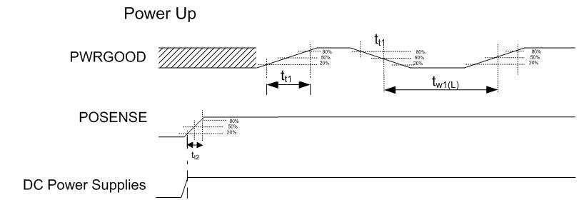 Figure 2. Power Up
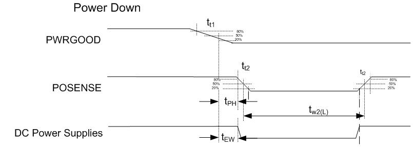 Figure 3. Power Down
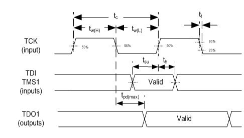 Figure 4. I/O Boundary Scan
 Figure 5. Programmable Output Clocks
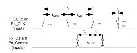 Figure 6. Port1, Port2, and Port3 Input Interface
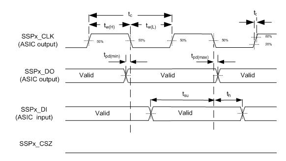 Figure 7. Synchronous Serial Port Interface - Master
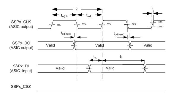 Figure 8. Synchronous Serial Port Interface - Slave
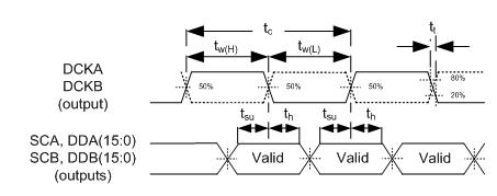 Figure 9. DMD LVDS Interface