SLLSEJ7 February 2015 DP83848-HT
PRODUCTION DATA.
- 1 Features
- 2 Applications
- 3 Description
- 4 Typical System Diagram
- 5 Revision History
- 6 Bare Die Information
- 7 Specifications
-
8 Detailed Description
- 8.1 Overview
- 8.2 Functional Block Diagram
- 8.3
Feature Description
- 8.3.1 100BASE-TX Transmitter
- 8.3.2 100BASE-TX Receiver
- 8.3.3
10BASE-T Transceiver Module
- 8.3.3.1 Operational Modes
- 8.3.3.2 Smart Squelch
- 8.3.3.3 Collision Detection and SQE
- 8.3.3.4 Carrier Sense
- 8.3.3.5 Normal Link Pulse Detection/Generation
- 8.3.3.6 Jabber Function
- 8.3.3.7 Automatic Link Polarity Detection and Correction
- 8.3.3.8 Transmit and Receive Filtering
- 8.3.3.9 Transmitter
- 8.3.3.10 Receiver
- 8.3.4 Reset Operation
- 8.4 Device Functional Modes
- 8.5 Programming
- 8.6
Register Maps
- 8.6.1 Register Block
- 8.6.2
Register Definition
- 8.6.2.1 Basic Mode Control Register (BMCR)
- 8.6.2.2 Basic Mode Status Register (BMSR)
- 8.6.2.3 PHY Identifier Register 1 (PHYIDR1)
- 8.6.2.4 PHY Identifier Register 2 (PHYIDR2)
- 8.6.2.5 Auto-Negotiation Advertisement Register (ANAR)
- 8.6.2.6 Auto-Negotiation Link Partner Ability Register (ANLPAR) (BASE Page)
- 8.6.2.7 Auto-Negotiation Link Partner Ability Register (ANLPAR) (Next Page)
- 8.6.2.8 Auto-Negotiate Expansion Register (ANER)
- 8.6.2.9 Auto-Negotiation Next Page Transmit Register (ANNPTR)
- 8.6.3
Extended Registers
- 8.6.3.1 PHY Status Register (PHYSTS)
- 8.6.3.2 MII Interrupt Control Register (MICR)
- 8.6.3.3 MII Interrupt Status and Miscellaneous Control Register (MISR)
- 8.6.3.4 False Carrier Sense Counter Register (FCSCR)
- 8.6.3.5 Receiver Error Counter Register (RECR)
- 8.6.3.6 100 Mb/s PCS Configuration and Status Register (PCSR)
- 8.6.3.7 RMII and Bypass Register (RBR)
- 8.6.3.8 LED Direct Control Register (LEDCR)
- 8.6.3.9 PHY Control Register (PHYCR)
- 8.6.3.10 10Base-T Status/Control Register (10BTSCR)
- 8.6.3.11 CD Test and BIST Extensions Register (CDCTRL1)
- 8.6.3.12 Energy Detect Control (EDCR)
- 9 Application and Implementation
- 10Power Supply Recommendations
- 11Layout
- 12Device and Documentation Support
- 13Mechanical, Packaging, and Orderable Information
Package Options
Mechanical Data (Package|Pins)
- KGD|0
Thermal pad, mechanical data (Package|Pins)
Orderable Information
1 Features
- Low-Power 3.3-V, 0.18-μm CMOS Technology
- Low Power Consumption <270 mW Typical
- 3.3-V MAC Interface
- Auto-MDIX for 10/100 Mb/s
- Energy Detection Mode
- 25-MHz Clock Out
- SNI Interface (Configurable)
- RMII Rev. 1.2 Interface (Configurable)
- MII Serial Management Interface (MDC and MDIO)
- IEEE 802.3u MII
- IEEE 802.3u Auto-Negotiation and Parallel Detection
- IEEE 802.3u ENDEC, 10BASE-T Transceivers and Filters
- IEEE 802.3u PCS, 100BASE-TX Transceivers and Filters
- IEEE 1149.1 JTAG
- Integrated ANSI X3.263 Compliant TP-PMD Physical Sublayer With Adaptive Equalization and Baseline Wander Compensation
- Error-Free Operation up to 150 Meters
- Programmable LED Support Link, 10 /100 Mb/s Mode, Activity, and Collision Detect
- Single Register Access for Complete PHY Status
- 10/100 Mb/s Packet BIST (Built-in Self Test)
- Supports Defense, Aerospace, and Medical Applications
- Controlled Baseline
- One Assembly and Test Site
- One Fabrication Site
- Extended Temperature Range (–55°C to 150°C)
- Extended Product Life Cycle
- Extended Product-Change Notification
- Product Traceability
2 Applications
- Automotive and Transportation
- Industrial Controls and Factory Automation
- General Embedded Applications
3 Description
The number of applications requiring ethernet connectivity continues to increase. Along with this increased market demand is a change in application requirements. The DP83848 was designed to allow ethernet connectivity in the harshest environments. This device is ideally suited for harsh environments for example wireless remote base stations, automotive, transportation and industrial control applications.
The DP83848 is a highly-reliable, feature-rich robust device which includes enhanced ESD protection, MII and RMII for maximum flexibility in MPU selection.
The DP83848 features integrated sublayers to support both 10BASE-T and 100BASE-TX Ethernet protocols, which ensures compatibility and interoperability with all other standards based Ethernet solutions.
Device Information(1)
| PART NUMBER | DIE | DIE SIZE (NOM) |
|---|---|---|
| DP83848-HT | KGD (49) | 1592 µm × 1532 µm |
- For all available packages, see the orderable addendum at the end of the data sheet.
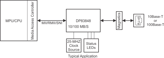
4 Typical System Diagram