SLLSEJ7 February 2015 DP83848-HT
PRODUCTION DATA.
- 1 Features
- 2 Applications
- 3 Description
- 4 Typical System Diagram
- 5 Revision History
- 6 Bare Die Information
- 7 Specifications
-
8 Detailed Description
- 8.1 Overview
- 8.2 Functional Block Diagram
- 8.3
Feature Description
- 8.3.1 100BASE-TX Transmitter
- 8.3.2 100BASE-TX Receiver
- 8.3.3
10BASE-T Transceiver Module
- 8.3.3.1 Operational Modes
- 8.3.3.2 Smart Squelch
- 8.3.3.3 Collision Detection and SQE
- 8.3.3.4 Carrier Sense
- 8.3.3.5 Normal Link Pulse Detection/Generation
- 8.3.3.6 Jabber Function
- 8.3.3.7 Automatic Link Polarity Detection and Correction
- 8.3.3.8 Transmit and Receive Filtering
- 8.3.3.9 Transmitter
- 8.3.3.10 Receiver
- 8.3.4 Reset Operation
- 8.4 Device Functional Modes
- 8.5 Programming
- 8.6
Register Maps
- 8.6.1 Register Block
- 8.6.2
Register Definition
- 8.6.2.1 Basic Mode Control Register (BMCR)
- 8.6.2.2 Basic Mode Status Register (BMSR)
- 8.6.2.3 PHY Identifier Register 1 (PHYIDR1)
- 8.6.2.4 PHY Identifier Register 2 (PHYIDR2)
- 8.6.2.5 Auto-Negotiation Advertisement Register (ANAR)
- 8.6.2.6 Auto-Negotiation Link Partner Ability Register (ANLPAR) (BASE Page)
- 8.6.2.7 Auto-Negotiation Link Partner Ability Register (ANLPAR) (Next Page)
- 8.6.2.8 Auto-Negotiate Expansion Register (ANER)
- 8.6.2.9 Auto-Negotiation Next Page Transmit Register (ANNPTR)
- 8.6.3
Extended Registers
- 8.6.3.1 PHY Status Register (PHYSTS)
- 8.6.3.2 MII Interrupt Control Register (MICR)
- 8.6.3.3 MII Interrupt Status and Miscellaneous Control Register (MISR)
- 8.6.3.4 False Carrier Sense Counter Register (FCSCR)
- 8.6.3.5 Receiver Error Counter Register (RECR)
- 8.6.3.6 100 Mb/s PCS Configuration and Status Register (PCSR)
- 8.6.3.7 RMII and Bypass Register (RBR)
- 8.6.3.8 LED Direct Control Register (LEDCR)
- 8.6.3.9 PHY Control Register (PHYCR)
- 8.6.3.10 10Base-T Status/Control Register (10BTSCR)
- 8.6.3.11 CD Test and BIST Extensions Register (CDCTRL1)
- 8.6.3.12 Energy Detect Control (EDCR)
- 9 Application and Implementation
- 10Power Supply Recommendations
- 11Layout
- 12Device and Documentation Support
- 13Mechanical, Packaging, and Orderable Information
Package Options
Mechanical Data (Package|Pins)
- KGD|0
Thermal pad, mechanical data (Package|Pins)
Orderable Information
9 Application and Implementation
NOTE
Information in the following applications sections is not part of the TI component specification, and TI does not warrant its accuracy or completeness. TI’s customers are responsible for determining suitability of components for their purposes. Customers should validate and test their design implementation to confirm system functionality.
9.1 Application Information
The DP83848 is a robust, full featured, low power, 10/100 Physical Layer devices. The DP83848 features integrated sublayers to support both 10BASE-T and 100BASE-TX Ethernet protocols, which ensure compatibility and interoperability with all other standards based Ethernet products in these applications:
- High-end peripheral devices
- Industrial controls
- Factor automation
- General embedded applications
9.2 Typical Application
 Figure 40. Typical Application Schematic
9.2.1 Design Requirements
9.2.1.1 Clock Requirements
DP83848 supports either an external CMOS-level oscillator source or a crystal resonator device. The X1 pin is the clock input, requiring either 25 or 50 MHz depending on the MII mode used. In MII mode (or RMII master mode in some products) either a 25-MHz crystal or 25-MHz oscillator may be used. For all PHYTER family products, the use of standard RMII mode (not RMII master mode) requires the use of a 50-MHz oscillator.
Table 59. 25-MHz Crystal Oscillator Requirements
| DESIGN PARAMETER | EXAMPLE VALUE |
|---|---|
| Frequency | 25/50 MHz |
| Frequency stability | ±50 ppm |
| Rise/fall time | Max 6 ns |
| Jitter (short term) | Max 800 ps |
| Jitter (long term) | Max 800 ps |
| Load capacitance | Minimum 15 pF |
| Symmetry | 40% to 60% |
| Logic 0 | Max 10% VDD, VDD = 3.3 V |
| Logic 1 | Min. 90% VDD, VDD = 3.3 V |
9.2.1.2 Magnetics
The magnetics have a large impact on the PHY performance as well. While several components are listed, others may be compatible following the requirements listed in Table 60. TI recommends that the magnetics include both an isolation transformer and an integrated common mode choke to reduce EMI.
Table 60. Magnetics Requirements
| DESIGN PARAMETER | EXAMPLE VALUE |
|---|---|
| Turn ratio | 1:1, ±2% |
| Insertion loss | –1 dB, 1 to 100 MHz |
| Return loss | –16 dB, 1 to 30 MHz |
| –12 dB, 30 to 60 MHz | |
| –10 dB, 60 to 80 MHz | |
| Differential to common rejection ration | –30 dB, 1 to 50 MHz |
| –20 dB, 50 to 150 MHz | |
| Crosstalk | –35 dB, 30 MHz |
| –30 dB, 60 MHz | |
| Isolation | 1500 Vrms |
9.2.2 Detailed Design Procedure
9.2.2.1 TPI Network Circuit
Figure 41 shows the recommended circuit for a 10/100 Mb/s twisted pair interface. The transmitter and the receiver of each node are DC isolated from the network cable by 1:1 transformers. A typical network configuration provides the services of autonegotiation, Auto-MDIX, 10-Mb/s operation, and 100-Mb/s operation. Autonegotiation is a feature which automatically determines the optimal network operating speed. Auto-MDIX is a feature allowing either straight-through or cross-over cables to be used. Autonegotiation uses link pulses to determine the operating mode. Link pulses appear as differential 2.5-V signals when ideal 50-Ω balanced loading is provided. 100 Mb/s data appears as 1 V, 0 V, and –1-V differential signals, and 10-Mb/s data appears as 2.5-V and –2.5-V differential signals across ideal loading. See Figure 44, Figure 45, and Figure 46.
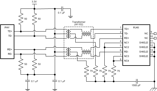 Figure 41. Typical 10/100 Mb/s Twisted Pair Interface
9.2.2.2 Clock In (X1) Requirements
The DP83848 supports an external CMOS level oscillator source or a crystal resonator device.
9.2.2.2.1 Oscillator
If an external clock source is used, X1 should be tied to the clock source and X2 should be left floating.
Specifications for CMOS oscillators: 25 MHz in MII Mode and 50 MHz in RMII Mode are listed in Table 61 and Table 62.
9.2.2.2.2 Crystal
A 25-MHz, parallel, 20-pF load crystal resonator should be used if a crystal source is desired. Figure 42 shows a typical connection for a crystal resonator circuit. The load capacitor values will vary with the crystal vendors; check with the vendor for the recommended loads.
The oscillator circuit is designed to drive a parallel resonance at cut crystal with a minimum drive level of 100 μW and a maximum of 500 μW. If a crystal is specified for a lower drive level, a current limiting resistor should be placed in series between X2 and the crystal.
As a starting point for evaluating an oscillator circuit, if the requirements for the crystal are not known, CL1 and CL2 should be set at 33 pF, and R1 should be set at 0 Ω.
Specification for 25 MHz crystal are listed in Table 63.
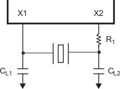 Figure 42. Crystal Oscillator Circuit
Table 61. 25-MHz Oscillator Specification
| PARAMETER | CONDITIONS | MIN | TYP | MAX | UNIT |
|---|---|---|---|---|---|
| Frequency | 25 | MHz | |||
| Frequency tolerance | Operational temperature | ±50 | ppm | ||
| Frequency stability | 1 year aging | ±50 | ppm | ||
| Rise/Fall time | 20% to 80% | 6 | ns | ||
| Jitter | Short term | 800(1) | ps | ||
| Jitter | Long term | 800(1) | ps | ||
| Symmetry | Duty cycle | 40% | 60% |
Table 62. 50 MHz Oscillator Specification
| PARAMETER | CONDITIONS | MIN | TYP | MAX | UNIT |
|---|---|---|---|---|---|
| Frequency | 50 | MHz | |||
| Frequency tolerance | Operational temperature | ±50 | ppm | ||
| Frequency stability | Operational temperature | ±50 | ppm | ||
| Rise/Fall time | 20% - 80% | 6 | ns | ||
| Jitter | Short term | 800(1) | ps | ||
| Jitter | Long term | 800(1) | ps | ||
| Symmetry | Duty cycle | 40% | 60% |
Table 63. 25 MHz Crystal Specification
| PARAMETER | CONDITIONS | MIN | TYP | MAX | UNIT |
|---|---|---|---|---|---|
| Frequency | 25 | MHz | |||
| Frequency tolerance | Operational temperature | ±50 | ppm | ||
| Frequency stability | 1 year aging | ±50 | ppm | ||
| Load capacitance | 25 | 40 | pF |
9.2.2.3 Power Feedback Circuit
To ensure correct operation for the DP83848, parallel caps with values of 10 μF (Tantalum) and 0.1 μF should be placed close to pin 23 (PFBOUT) of the device.
Pin 18 (PFBIN1) and pin 37 (PFBIN2) must be connected to pin 23 (PFBOUT), each pin requires a small capacitor (.1 μF). See Figure 43 for proper connections.
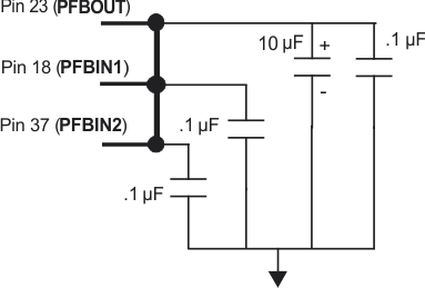 Figure 43. Power Feedback Connection
9.2.2.4 Power Down and Interrupt
The power down and interrupt functions are multiplexed on pin 7 of the device. By default, this pin functions as a power down input and the interrupt function is disabled. Setting bit 0 (INT_OE) of MICR (0x11h) will configure the pin as an active low interrupt output.
9.2.2.4.1 Power-Down Control Mode
The PWR_DOWN/INT pin can be asserted low to put the device in a power down mode. This is equivalent to setting bit 11 (power down) in the basic mode control register, BMCR (0x00h). An external control signal can be used to drive the pin low, overcoming the weak internal pull-up resistor. Alternatively, the device can be configured to initialize into a power down state by use of an external pulldown resistor on the PWR_DOWN/INT pin. Since the device will still respond to management register accesses, setting the INT_OE bit in the MICR register will disable the PWR_DOWN/INT input, allowing the device to exit the power down state.
9.2.2.4.2 Interrupt Mechanisms
The interrupt function is controlled via register access. All interrupt sources are disabled by default. Setting bit 1 (INTEN) of MICR (0x11h) will enable interrupts to be output, dependent on the interrupt mask set in the lower byte of the MISR (0x12h). The PWR_DOWN/INT pin is asynchronously asserted low when an interrupt condition occurs. The source of the interrupt can be determined by reading the upper byte of the MISR. One or more bits in the MISR will be set, denoting all currently pending interrupts. Reading of the MISR clears ALL pending interrupts.
Example: To generate an interrupt on a change of link status or on a change of energy detect power state, the steps would be:
- Write 0003h to MICR to set INTEN and INT_OE
- Write 0060h to MISR to set ED_INT_EN and LINK_INT_EN
- Monitor PWR_DOWN/INT pin
When PWR_DOWN/INT pin asserts low, user would read the MISR register to see if the ED_INT or LINK_INT bits are set, i.e. which source caused the interrupt. After reading the MISR, the interrupt bits should clear and the PWR_DOWN/INT pin will deassert.
9.2.2.5 Energy Detect Mode
When energy detect is enabled and there is no activity on the cable, the DP83848 will remain in a low power mode while monitoring the transmission line. Activity on the line will cause the DP83848 to go through a normal power up sequence. Regardless of cable activity, the DP83848 will occasionally wake up the transmitter to put ED pulses on the line, but will otherwise draw as little power as possible. Energy detect functionality is controlled via register energy detect control (EDCR), address 0x1Dh.
9.2.3 Application Curves
Transformers provide the functions of DC isolation from the cable, and DC biasing at the physical layer device. Isolation is necessary to meet IEEE 802.3 AC and DC isolation specifications for cabled configurations. IEEE 802.3 isolation requirements are described in section 14.3.1.1 of the specification, and include the ability to sustain cable faults to 1500-V 50- or 60-Hz or 2250-Vdc voltage levels for 60 s. PHYTER product transmitters and receivers are DC biased internally, from the transformer centertap, and through 50-Ω load resistors used in typical applications.
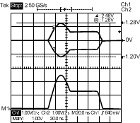 Figure 44. Sample Link Pulse Waveform
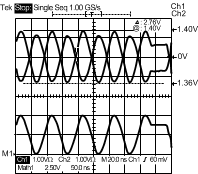 Figure 46. Sample 10-Mb/s Waveform
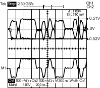 Figure 45. Sample 100-Mb/s Waveform (MLT-3)