SLVSDD5 August 2017 DRV5012
PRODUCTION DATA.
- 1 Features
- 2 Applications
- 3 Description
- 4 Revision History
- 5 Pin Configuration and Functions
- 6 Specifications
- 7 Detailed Description
- 8 Application and Implementation
- 9 Power Supply Recommendations
- 10Layout
- 11Device and Documentation Support
- 12Mechanical, Packaging, and Orderable Information
Package Options
Refer to the PDF data sheet for device specific package drawings
Mechanical Data (Package|Pins)
- DMR|4
Thermal pad, mechanical data (Package|Pins)
- DMR|4
Orderable Information
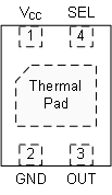
5 Pin Configuration and Functions
DMR Package
4-Pin X2SON With Exposed Thermal Pad
Top View

Pin Functions
| PIN | I/O | DESCRIPTION | |
|---|---|---|---|
| NAME | NO. | ||
| GND | 2 | — | Ground reference |
| OUT | 3 | O | Push-pull CMOS output. Drives a VCC or ground level. |
| SEL | 4 | I | CMOS input that selects the sampling rate: a low voltage sets 20 Hz; a high voltage sets 2.5 kHz. |
| VCC | 1 | — | 1.65-V to 5.5-V power supply. TI recommends connecting this pin to a ceramic capacitor to ground with a value of at least 0.1 µF. |
| Thermal Pad | PAD | — | No-connect. This pin should be left floating or tied to ground. It should be soldered to the board for mechanical support. |