SLVSA73F April 2010 – July 2014 DRV8825
PRODUCTION DATA.
- 1 Features
- 2 Applications
- 3 Description
- 4 Simplified Schematic
- 5 Revision History
- 6 Pin Configuration and Functions
- 7 Specifications
- 8 Detailed Description
- 9 Application and Implementation
- 10Power Supply Recommendations
- 11Layout
- 12Device and Documentation Support
- 13Mechanical, Packaging, and Orderable Information
Package Options
Mechanical Data (Package|Pins)
- PWP|28
Thermal pad, mechanical data (Package|Pins)
- PWP|28
Orderable Information
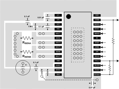
11 Layout
11.1 Layout Guidelines
The VMA and VMB pins should be bypassed to GND using low-ESR ceramic bypass capacitors with a recommended value of 0.1-μF rated for VMx. This capacitor should be placed as close to the VMA and VMB pins as possible with a thick trace or ground plane connection to the device GND pin.
The VMA and VMB pins must be bypassed to ground using an appropriate bulk capacitor. This component may be an electrolytic and should be located close to the DRV8825.
A low-ESR ceramic capacitor must be placed in between the CPL and CPH pins. TI recommends a value of 0.01-μF rated for VMx. Place this component as close to the pins as possible.
A low-ESR ceramic capacitor must be placed in between the VMA and VCP pins. TI recommends a value of 0.1-μF rated for 16 V. Place this component as close to the pins as possible. Also, place a 1-MΩ resistor between VCP and VMA.
Bypass V3P3 to ground with a ceramic capacitor rated 6.3 V. Place this bypass capacitor as close to the pin as possible
11.2 Layout Example
11.3 Thermal Protection
The DRV8825 has thermal shutdown (TSD) as described above. If the die temperature exceeds approximately 150°C, the device will be disabled until the temperature drops to a safe level.
Any tendency of the device to enter TSD is an indication of either excessive power dissipation, insufficient heatsinking, or too high an ambient temperature.
11.3.1 Power Dissipation
Power dissipation in the DRV8825 is dominated by the power dissipated in the output FET resistance, or RDS(ON). Average power dissipation when running a stepper motor can be roughly estimated by Equation 5.
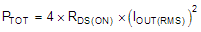
where PTOT is the total power dissipation, RDS(ON) is the resistance of each FET, and IOUT(RMS) is the RMS output current being applied to each winding. IOUT(RMS) is equal to the approximately 0.7x the full-scale output current setting. The factor of 4 comes from the fact that there are two motor windings, and at any instant two FETs are conducting winding current for each winding (one high-side and one low-side).
The maximum amount of power that can be dissipated in the device is dependent on ambient temperature and heatsinking.
Note that RDS(ON) increases with temperature, so as the device heats, the power dissipation increases. This must be taken into consideration when sizing the heatsink.
11.3.2 Heatsinking
The PowerPAD™ package uses an exposed pad to remove heat from the device. For proper operation, this pad must be thermally connected to copper on the PCB to dissipate heat. On a multi-layer PCB with a ground plane, this can be accomplished by adding a number of vias to connect the thermal pad to the ground plane. On PCBs without internal planes, copper area can be added on either side of the PCB to dissipate heat. If the copper area is on the opposite side of the PCB from the device, thermal vias are used to transfer the heat between top and bottom layers.
For details about how to design the PCB, refer to TI application report SLMA002, "PowerPAD™ Thermally Enhanced Package" and TI application brief SLMA004, PowerPAD™ Made Easy, available at www.ti.com.
In general, the more copper area that can be provided, the more power can be dissipated. It can be seen that the heatsink effectiveness increases rapidly to about 20 cm2, then levels off somewhat for larger areas.