SNLS336J October 2010 – November 2014 DS90UH925Q-Q1
PRODUCTION DATA.
- 1 Features
- 2 Applications
- 3 Description
- 4 Revision History
- 5 Pin Configuration and Functions
-
6 Specifications
- 6.1 Absolute Maximum Ratings
- 6.2 Handling Ratings
- 6.3 Recommended Operating Conditions
- 6.4 Thermal Information
- 6.5 DC Electrical Characteristics
- 6.6 AC Electrical Characteristics
- 6.7 DC and AC Serial Control Bus Characteristics
- 6.8 Recommended Timing for Serial Control Bus
- 6.9 Switching Characteristics
- 6.10 Typical Charateristics
-
7 Detailed Description
- 7.1 Overview
- 7.2 Functional Block Diagram
- 7.3
Feature Description
- 7.3.1 High Speed Forward Channel Data Transfer
- 7.3.2 Low Speed Back Channel Data Transfer
- 7.3.3 Backward Compatible Mode
- 7.3.4 Common Mode Filter Pin (CMF)
- 7.3.5 Video Control Signal Filter
- 7.3.6 Power Down (PDB)
- 7.3.7 Remote Auto Power Down Mode
- 7.3.8 LVCMOS VDDIO Option
- 7.3.9 Input PCLK Loss Detect
- 7.3.10 Serial Link Fault Detect
- 7.3.11 Pixel Clock Edge Select (RFB)
- 7.3.12 Low Frequency Optimization (LFMODE)
- 7.3.13 Interrupt Pin — Functional Description and Usage (INTB)
- 7.3.14 EMI Reduction Features
- 7.4 Device Functional Modes
- 7.5 Programming
- 7.6 Register Maps
- 8 Applications and Implementation
- 9 Power Supply Recommendations
- 10Layout
- 11Device and Documentation Support
- 12Mechanical, Packaging, and Orderable Information
Package Options
Mechanical Data (Package|Pins)
- RHS|48
Thermal pad, mechanical data (Package|Pins)
- RHS|48
Orderable Information
1 Features
- Integrated HDCP Cipher Engine with On-chip Key Storage
- Bidirectional Control Interface Channel Interface with I2C Compatible Serial Control Bus
- Supports High Definition (720p) Digital Video Format
- RGB888 + VS, HS, DE and I2S Audio Supported
- 5 to 85 MHz PCLK Supported
- Single 3.3V Operation with 1.8 V or 3.3 V Compatible LVCMOS I/O Interface
- AC-coupled STP Interconnect up to 10 meters
- Parallel LVCMOS Video Inputs
- DC-balanced & Scrambled Data with Embedded Clock
- HDCP Content Protected
- Supports HDCP Repeater Application
- Internal Pattern Generation
- Low Power Modes Minimize Power Dissipation
- Automotive Grade Product: AEC-Q100 Grade 2 Qualified
- > 8k V HBM and ISO 10605 ESD rating
- Backward Compatible Modes
2 Applications
- Automotive Display for Navigation
- Rear Seat Entertainment Systems
3 Description
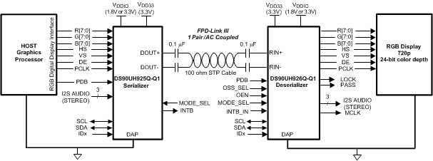
The DS90UH925Q-Q1 serializer, in conjunction with the DS90UH926Q-Q1 deserializer, provides a solution for secure distribution of content-protected digital video within automotive entertainment systems. This chipset translates a parallel RGB Video Interface into a single pair high-speed serialized interface. The digital video data is protected using the industry standard HDCP copy protection scheme. The serial bus scheme, FPD-Link III, supports video and audio data transmission and full duplex control including I2C communication over a single differential link. Consolidation of video data and control over a single differential pair reduces the interconnect size and weight, while also eliminating skew issues and simplifying system design.
The DS90UH925Q-Q1 serializer embeds the clock, content protects the data payload, and level shifts the signals to high-speed low voltage differential signaling. Up to 24 RGB data bits are serialized along with three video control signals and up to two I2S data inputs.
EMI is minimized by the use of low voltage differential signaling, data scrambling and randomization and spread spectrum clocking compatibility.
The HDCP cipher engine is implemented in the serializer and deserializer. HDCP keys are stored in on-chip memory.
Device Information(1)
| PART NUMBER | PACKAGE | BODY SIZE |
|---|---|---|
| DS90UH925Q-Q1 | WQFN (48) | 7.00 mm x 7.00 mm |
Simplified Schematic