SLVSE49A July 2017 – July 2017 ESD401
PRODUCTION DATA.
- 1 Features
- 2 Applications
- 3 Description
- 4 Revision History
- 5 Pin Configuration and Functions
- 6 Specifications
- 7 Detailed Description
- 8 Application and Implementation
- 9 Power Supply Recommendations
- 10Layout
- 11Device and Documentation Support
- 12Mechanical, Packaging, and Orderable Information
Package Options
Mechanical Data (Package|Pins)
- DPY|2
Thermal pad, mechanical data (Package|Pins)
- DPY|2
Orderable Information
7 Detailed Description
7.1 Overview
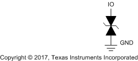
The ESD401 is a bidirectional ESD Protection Diode with ultra-low clamping voltage. This device can dissipate ESD strikes above the maximum level specified by the IEC 61000-4-2 International Standard. The ultra-low clamping makes this device ideal for protecting any sensitive signal pins.
7.2 Functional Block Diagram

7.3 Feature Description
7.3.1 IEC 61000-4-2 ESD Protection
The I/O pins can withstand ESD events up to ±24-kV contact and ±30-kV air gap. An ESD-surge clamp diverts the current to ground.
7.3.2 IEC 61000-4-4 EFT Protection
The I/O pins can withstand an electrical fast transient burst of up to 80 A (5/50 ns waveform, 4 kV with 50-Ω impedance). An ESD-surge clamp diverts the current to ground.
7.3.3 IEC 61000-4-5 Surge Protection
The I/O pins can withstand surge events up to 4.5 A and 67W (8/20 µs waveform). An ESD-surge clamp diverts this current to ground.
7.3.4 IO Capacitance
The capacitance between each I/O pin to ground is 0.77 pF (typical) and 0.95 pF (maximum).
7.3.5 DC Breakdown Voltage
The DC breakdown voltage of each I/O pin is ±8.3 V typical. This ensures that sensitive equipment is protected from surges above the reverse standoff voltage of ±5.5 V.
7.3.6 Low Leakage Current
The I/O pins feature an low leakage current of 10 nA (maximum) with a bias of ±2.5 V.
7.3.7 Low ESD Clamping Voltage
The I/O pins feature an ESD clamp that is capable of clamping the voltage to 24 V (TLP IPP = 16 A).
7.3.8 Industrial Temperature Range
This device features an industrial operating range of –40°C to +125°C.
7.3.9 Industry Standard Footprint
The layout of this device makes it simple and easy to add protection to an existing layout. The packages offers flow-through routing, requiring minimal modification to an existing layout.
7.4 Device Functional Modes
The ESD401 is a passive integrated circuit that triggers when voltages are above VBRF or below VBRR. During ESD events, voltages as high as ±24 kV (contact) or ±30 kV ( air) can be directed to ground via the internal diode network. When the voltages on the protected line fall below the trigger levels of ESD401 (usually within 10s of nano-seconds) the device reverts to passive.
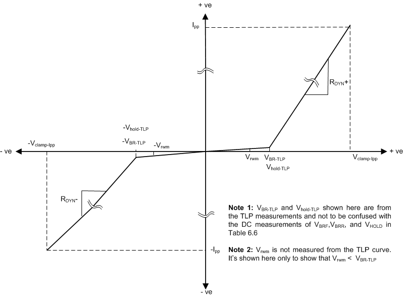
Figure 11 shows typical TLP behavior of bi-directional ESD device that does not exhibit snapback.
 Figure 11. Typical TlpLP Behavior Of Bi-directional ESD Device that Does Not Exhibit Snapback