SNOSCZ5A June 2015 – June 2015 FDC2112 , FDC2114 , FDC2212 , FDC2214
PRODUCTION DATA.
- 1 Features
- 2 Applications
- 3 Description
- 4 Revision History
- 5 Description, continued
- 6 Device Comparison Table
- 7 Pin Configuration and Functions
- 8 Specifications
-
9 Detailed Description
- 9.1 Overview
- 9.2 Functional Block Diagrams
- 9.3 Feature Description
- 9.4 Device Functional Modes
- 9.5 Programming
- 9.6
Register Maps
- 9.6.1 Register List
- 9.6.2 Address 0x00, DATA_CH0
- 9.6.3 Address 0x01, DATA_LSB_CH0 (FDC2212 / FDC2214 only)
- 9.6.4 Address 0x02, DATA_CH1
- 9.6.5 Address 0x03, DATA_LSB_CH1 (FDC2212 / FDC2214 only)
- 9.6.6 Address 0x04, DATA_CH2 (FDC2114, FDC2214 only)
- 9.6.7 Address 0x05, DATA_LSB_CH2 (FDC2214 only)
- 9.6.8 Address 0x06, DATA_CH3 (FDC2114, FDC2214 only)
- 9.6.9 Address 0x07, DATA_LSB_CH3 (FDC2214 only)
- 9.6.10 Address 0x08, RCOUNT_CH0
- 9.6.11 Address 0x09, RCOUNT_CH1
- 9.6.12 Address 0x0A, RCOUNT_CH2 (FDC2114, FDC2214 only)
- 9.6.13 Address 0x0B, RCOUNT_CH3 (FDC2114, FDC2214 only)
- 9.6.14 Address 0x0C, OFFSET_CH0 (FDC21112 / FDC2114 only)
- 9.6.15 Address 0x0D, OFFSET_CH1 (FDC21112 / FDC2114 only)
- 9.6.16 Address 0x0E, OFFSET_CH2 (FDC2114 only)
- 9.6.17 Address 0x0F, OFFSET_CH3 (FDC2114 only)
- 9.6.18 Address 0x10, SETTLECOUNT_CH0
- 9.6.19 Address 0x11, SETTLECOUNT_CH1
- 9.6.20 Address 0x12, SETTLECOUNT_CH2 (FDC2114, FDC2214 only)
- 9.6.21 Address 0x13, SETTLECOUNT_CH3 (FDC2114, FDC2214 only)
- 9.6.22 Address 0x14, CLOCK_DIVIDERS_CH0
- 9.6.23 Address 0x15, CLOCK_DIVIDERS_CH1
- 9.6.24 Address 0x16, CLOCK_DIVIDERS_CH2 (FDC2114, FDC2214 only)
- 9.6.25 Address 0x17, CLOCK_DIVIDERS_CH3 (FDC2114, FDC2214 only)
- 9.6.26 Address 0x18, STATUS
- 9.6.27 Address 0x19, ERROR_CONFIG
- 9.6.28 Address 0x1A, CONFIG
- 9.6.29 Address 0x1B, MUX_CONFIG
- 9.6.30 Address 0x1C, RESET_DEV
- 9.6.31 Address 0x1E, DRIVE_CURRENT_CH0
- 9.6.32 Address 0x1F, DRIVE_CURRENT_CH1
- 9.6.33 Address 0x20, DRIVE_CURRENT_CH2 (FDC2114 / FDC2214 only)
- 9.6.34 Address 0x21, DRIVE_CURRENT_CH3 (FDC2114 / FDC2214 only)
- 9.6.35 Address 0x7E, MANUFACTURER_ID
- 9.6.36 Address 0x7F, DEVICE_ID
- 10Application and Implementation
- 11Power Supply Recommendations
- 12Layout
- 13Device and Documentation Support
- 14Mechanical, Packaging, and Orderable Information
Package Options
Mechanical Data (Package|Pins)
- DNT|12
Thermal pad, mechanical data (Package|Pins)
Orderable Information
10 Application and Implementation
NOTE
Information in the following applications sections is not part of the TI component specification, and TI does not warrant its accuracy or completeness. TI’s customers are responsible for determining suitability of components for their purposes. Customers should validate and test their design implementation to confirm system functionality.
10.1 Application Information
10.1.1 Sensor Configuration
The FDC supports two sensor configurations. Both configurations use an LC tank to set the frequency of oscillation. A typical choice is an 18 μH shielded SMD inductor in parallel with a 33 pF capacitor, which result in a 6.5 MHz oscillation frequency. In the single-ended configuration in Figure 54, a conductive plate is connected IN0A. Together with a target object, the conductive plate forms a variable capacitor.
 Figure 54. Single-ended Sensor Configuration
In the differential sensor configuration in Figure 55, one conductive plate is connected to IN0A, and a second conductive plate is connected to IN0B. Together, they form a variable capacitor. When using an single-ended sensor configuration, set CHx_FIN_SEL to b10 (divide by 2).
 Figure 55. Differential Sensor Configuration
The single-ended configuration allows higher sensing range than the differential configuration for a given total sensor plate area. In applications in which high sensitivity at close proximity is desired, the differential configuration performs better than the single-ended configuration.
10.1.2 Shield
in order to minimize interference from external objects, some applications require an additional plate which acts as a shield. The shield can either be:
- actively driven shield: The shield is a buffered signal of the INxA pin. The signal is buffered by an external amplifier with a gain of 1.
- passive shield: The shield is connected to GND. Adding a passive shield decreases sensitivity of the sensor, but is dependent on the distance between the distance between the sensing plate and the shield. The distance between the sensing plate and the shield should be adjusted to achieve the required sensitivity
10.2 Typical Application
The FDC can be used to measure liquid level in non-conductive containers. Due to its very high excitation rate capability, it is able to measure soapy water, ink, soap, and other conductive liquids. Capacitive sensors can be attached to the outside of the container or be located remotely from the container, allowing for contactless measurements.
The working principle is based on a ratiometric measurement; Figure 56 shows a possible system implementation which uses three electrodes. The Level electrode provides a capacitance value proportional to the liquid level. The Reference Environmental electrode and the Reference Liquid electrode are used as references. The Reference Liquid electrode accounts for the liquid dielectric constant and its variation, while the Reference Environmental electrode is used to compensate for any other environmental variations that are not due to the liquid itself. Note that the Reference Environmental electrode and the Reference Liquid electrode are the same physical size (hREF).
For this application, single-ended measurements on the active channels are appropriate, as the tank is grounded. Use to determine the liquid level from the measured capacitances:

where
- CRE is the capacitance of the Reference Environmental electrode,
- CRL is the capacitance of the Reference Liquid electrode,
- CLev is the current value of the capacitance measured at the Level electrode sensor,
- CLev(0) is the capacitance of the Level electrode when the container is empty, and
- hREF is the height in the desired units of the Container or Liquid Reference electrodes.
The ratio between the capacitance of the level and the reference electrodes allows simple calculation of the liquid level inside the container itself. Very high sensitivity values (that is, many LSB/mm) can be obtained due to the high resolution of the FDC2x1x, even when the sensors are located remotely from the container. Note that this approach assumes that the container has a uniform cross section from top to bottom, so that each incremental increase or decrease in the liquid represents a change in volume that is directly related to the height of the liquid.
10.2.1 Schematic
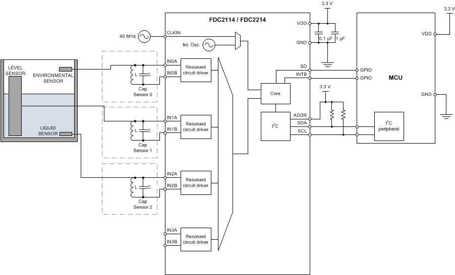 Figure 56. FDC (Liquid Level Measurement)
10.2.2 Design Requirements
The liquid level measurement should be independent of the liquid, which can be achieved using the 3-electrode design described above. Moreover, the sensor should be isolated from environmental interferers such as a human body, other objects, or EMI.
10.2.3 Detailed Design Procedure
In capacitive sensing systems, the design of the sensor plays an important role in determining system performance and capabilities. In most cases the sensor is simply a metal plate that can be designed on the PCB.
The sensor used in this example is implemented with a two-layer PCB. On the top layer, which faces the tank, there are the 3 electrodes (Reference Environmental, Reference Liquid, and Level) with a ground plane surrounding the electrodes.
Depending on the shape of the container, the FDC can be located on the sensor PCB to minimize the length of the traces between the input channels and the sensors. In case the shape of the container or other mechanical constraints do not allow having the sensors and the FDC on the same PCB, the traces which connect the channels to the sensor need to be shielded with the appropriate shield.
10.2.3.1 Application Performance Plot
A liquid level sensor with 3 electrodes like the one shown in the schematic was connected to the EVM. The plot shows the capacitance measured by Level sensor at different levels of liquid in the tank. The capacitance of the Reference Liquid and Reference Environmental sensors have a steady value because they experience consistent exposure to liquid and air, while the capacitance of the level sensor (Level) increases linearly with the height of the liquid in the tank.
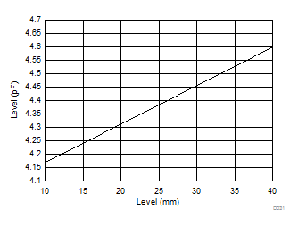 Figure 57. Electrodes' Capacitance vs. Liquid Level
10.2.3.2 Recommended Initial Register Configuration Values
The application requires 100SPS ( TSAMPLE = 10 ms). A sensor with an 18µH inductor and a 33pF capacitor is used. Additional pin, trace, and wire capacitance accounts for 20pF, so the total capacitance is 53pF.
Using L and C, fSENSOR = 1/2π√(LC) = 1/2π√(18*10-6 * 50*10-12) = 5.15 MHz. This represents the maximum sensor frequency. When the sensor capacitance is added, the frequency will decrease.
Using a system master clock of 40 MHz applied to the CLKIN pin allows flexibility for setting the internal clock frequencies. The sensor coils are connected to channel 0 (IN0A and IN0B pins), channel 1 (IN1A and IN1B pins), and channel 2 (IN2A and IN2B pins).
After powering on the FDC, it will be in Sleep Mode. Program the registers as follows (example sets registers for channel 0 only; channel 1 and channel 2 registers can use equivalent configuration):
- Set the dividers for channel 0.
- Because the sensor is in an single-ended configuration, the sensor frequency select register should be set to 2, which means setting field CH0_FIN_SELto b10.
- The design constraint for fREF0 is > 4 × fSENSOR. To satisfy this constraint, fREF0 must be greater than 20.6 MHz, so the reference divider should be set to 1. This is done by setting the CH0_FREF_DIVIDER field to 0x01.
- The combined value for Chan. 0 divider register (0x14) is 0x2001.
- Sensor drive current: to ensure that the oscillation amplitude is between 1.2V and 1.8V, measure the oscillation amplitude on an oscilloscope and adjust the IDRIVE value, or use the integrated FDC GUI feature to determine the optimal setting. In this case the IDRIVE value should be set to 15 (decimal), which results in an oscillation amplitude of 1.68 V(pk). The INIT_DRIVE current field should be set to 0x00. The combined value for the DRIVE_CURRENT_CH0 register (addr 0x1E) is 0x7C00.
- Program the settling time for Channel 0 (see Multi-Channel and Single-Channel Operation).
- CHx_SETTLECOUNT > Vpk × fREFx × C × π2 / (32 × IDRIVEX) → 7.5, rounded up to 8. To provide margin to account for system tolerances, a higher value of 10 is chosen.
- Register 0x10 should be programmed to a minimum of 10.
- The settle time is: (10 x 16)/40,000,000 = 4 µs
- The value for Chan. 0 SETTLECOUNT register (0x10) is 0x000A.
- The channel switching delay is ~1μs for fREF = 40 MHz (see Multi-Channel and Single-Channel Operation)
- Set the conversion time by the programming the reference count for Channel 0. The budget for the conversion time is : 1/N * (TSAMPLE – settling time – channel switching delay) = 1/3 (10,000 – 4 – 1) = 3.33 ms
- To determine the conversion time register value, use the following equation and solve for CH0_RCOUNT: Conversion Time (tC0)= (CH0_RCOUNTˣ16)/fREF0.
- This results in CH0_RCOUNT having a value of 8329 decimal (rounded down). Note that this yields an ENOB > 13 bits.
- Set the CH0_RCOUNT register (0x08) to 0x2089.
- Use the default values for the ERROR_CONFIG register (address 0x19). By default, no interrupts are enabled
- Program the MUX_CONFIG register
- Set the AUTOSCAN_EN to b1 bit to enable sequential mode
- Set RR_SEQUENCE to b10 to enable data conversion on three channels (channel 0, channel 1, channel 2)
- Set DEGLITCH to b101 to set the input deglitch filter bandwidth to 10MHz, the lowest setting that exceeds the oscillation tank frequency.
- The combined value for the MUX_CONFIG register (address 0x1B) is 0xC20D
- Finally, program the CONFIG register as follows:
- Set the ACTIVE_CHAN field to b00 to select channel 0.
- Set SLEEP_MODE_EN field to b0 to enable conversion.
- Set SENSOR_ACTIVATE_SEL = b0, for full current drive during sensor activation
- Set the REF_CLK_SRC field to b1 to use the external clock source.
- Set the other fields to their default values.
- The combined value for the CONFIG register (address 0x1A) is 0x1601.
We then read the conversion results for channel 0 to channel 2 every 10ms from register addresses 0x00 to 0x05.
Based on the example configuration above, the following register write sequence is recommended:
Table 47. Recommended Initial Register Configuration Values (Multi-channel Operation)
| ADDRESS | VALUE | REGISTER NAME | COMMENTS |
|---|---|---|---|
| 0x08 | 0x8329 | RCOUNT_CH0 | Reference count calculated from timing requirements (100 SPS) and resolution requirements |
| 0x09 | 0x8329 | RCOUNT_CH1 | Reference count calculated from timing requirements (100 SPS) and resolution requirements |
| 0x0A | 0x8329 | RCOUNT_CH2 | Reference count calculated from timing requirements (100 SPS) and resolution requirements |
| 0x10 | 0x000A | SETTLECOUNT_CH0 | Minimum settling time for chosen sensor |
| 0x11 | 0x000A | SETTLECOUNT_CH1 | Minimum settling time for chosen sensor |
| 0x12 | 0x000A | SETTLECOUNT_CH2 | Minimum settling time for chosen sensor |
| 0x14 | 0x2002 | CLOCK_DIVIDER_CH0 | CH0_FIN_DIVIDER = 1, CH0_FREF_DIVIDER = 2 |
| 0x15 | 0x2002 | CLOCK_DIVIDER_CH1 | CH1_FIN_DIVIDER = 1, CH1_FREF_DIVIDER = 2 |
| 0x16 | 0x2002 | CLOCK_DIVIDER_CH2 | CH1_FIN_DIVIDER = 1, CH1_FREF_DIVIDER = 2 |
| 0x19 | 0x0000 | ERROR_CONFIG | Can be changed from default to report status and error conditions |
| 0x1B | 0xC20D | MUX_CONFIG | Enable Ch 0 , Ch 1, and Ch 2 (sequential mode), set Input deglitch bandwidth to 10MHz |
| 0x1E | 0x7C00 | DRIVE_CURRENT_CH0 | Sets sensor drive current on ch 0 |
| 0x1F | 0x7C00 | DRIVE_CURRENT_CH1 | Sets sensor drive current on ch 1 |
| 0x20 | 0x7C00 | DRIVE_CURRENT_CH2 | Sets sensor drive current on ch 2 |
| 0x1A | 0x1601 | CONFIG | enable full current drive during sensor activation, select external clock source, wake up device to start conversion. This register write must occur last because device configuration is not permitted while the FDC is in active mode. |
10.2.3.3 Inductor Self-Resonant Frequency
Every inductor has a distributed parasitic capacitance, which is dependent on construction and geometry. At the Self-Resonant Frequency (SRF), the reactance of the inductor cancels the reactance of the parasitic capacitance. Above the SRF, the inductor will electrically appear to be a capacitor. Because the parasitic capacitance is not well-controlled or stable, it is recommended that: fSENSOR < 0.8 × fSR.
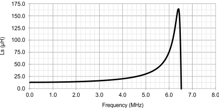 Figure 58. Example Coil Inductance vs. Frequency
The example inductor in Figure 58, has a SRF at 6.38 MHz; therefore the inductor should not be operated above 0.8×6.38 MHz, or 5.1 MHz.
10.2.4 Application Curves
Common test conditions (unless specified otherwise): Sensor capacitor: 1 layer, 20.9 x 13.9 mm, Bourns CMH322522-180KL sensor inductor with L=18 µH and 33 pF 1% COG/NP0 Target: Grounded aluminum plate (176 x 123 mm), Channel = Channel 0 (continuous mode) CLKIN = 40 MHz, CHx_FIN_SEL = b10, CHx_FREF_DIVIDER = b00 0000 0001 CH0_RCOUNT = 0xFFFF, SETTLECOUNT_CH0 = 0x0100, DRIVE_CURRENT_CH0 = 0x7800
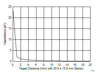 Figure 59. FDC2212 / FDC2214: Capacitance vs. Target Distance (0 to 20mm)
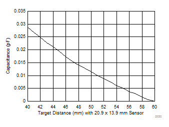 Figure 61. FDC2212 / FDC2214: Capacitance vs. Target Distance (40 to 60mm)
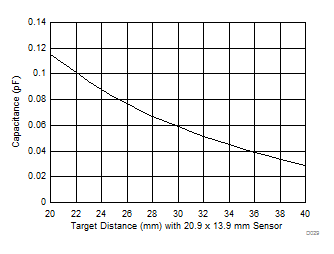 Figure 60. FDC2112 / FDC2114: Capacitance vs. Target Distance (20 to 40mm)
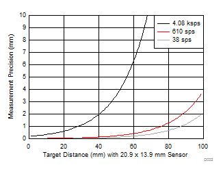 Figure 62. Measurement precision in Distance vs. Target Distance (0 to 60mm)
10.2.5 Power-Cycled Applications
For applications which do not require high sample rates or maximum conversion resolution, the total active conversion time of the FDC can be minimized to reduce power consumption. This can be done by either by using sleep mode or shutdown mode during times in which conversions are not required (see Device Functional Modes).
As an example, for an application which only needs 10 samples per second with a resolution of 16 bits can utilize the low-power modes. The sensor requires SETTLECOUNT = 16 and IDRIVE of 01111b (0.146 mA). Given FREF = 40 MHz and RCOUNT = 4096 will provide the resolution required. This corresponds to 4096 * 16 * 10 / 40 MHz → 16.4 ms of active conversion time per second. Start-up time and channel switch delay account for an additional 0.34 ms. For the remainder of the time, the device can be in sleep mode: Therefore, the average current is 19.4 ms * 3.6 mA active current + 980.6 ms of 35 µA of sleep current, which is approximately 104.6 µA of average supply current. Sleep mode retains register settings and therefore requires less I2C writes to wake up the FDC than shutdown mode.
Greater current savings can be realized by use of shutdown mode during inactive periods. In shutdown mode, device configuration is not retained, and so the device must be configured for each sample. For this example, configuring each sample takes approximately 1.2 ms (13 registers * 92.5 µs per register). The total active time is 20.6 ms. The average current is 20 ms * 3.6 mA active current + 980 ms * 2 µA of shutdown current, which is approximately 75 µA of average supply current.
10.3 Do's and Don'ts
- Do leave a small gap between sensor plates in differential configurations. 2-3mm minimum separation is recommended.
- The FDC does not support hot-swapping of the sensors. Do not hot-swap sensors, for example by using external multiplexers.