SBOS790 April 2017 INA233
PRODUCTION DATA.
- 1 Features
- 2 Applications
- 3 Description
- 4 Revision History
- 5 Pin Configuration and Functions
- 6 Specifications
-
7 Detailed Description
- 7.1 Overview
- 7.2 Functional Block Diagram
- 7.3 Feature Description
- 7.4 Device Functional Modes
- 7.5 Programming
- 7.6
Register Maps
- 7.6.1 PMBus Command Support
- 7.6.2
Standard PMBus Commands
- 7.6.2.1 CLEAR_FAULTS (03h)
- 7.6.2.2 RESTORE_DEFAULT_ALL (12h)
- 7.6.2.3 CAPABILITY (19h)
- 7.6.2.4 IOUT_OC_WARN_LIMIT (4Ah) [default = 01111111 11111000]
- 7.6.2.5 VIN_OV_WARN_LIMIT (57h) [default = 01111111 11111000]
- 7.6.2.6 VIN_UV_WARN_LIMIT (58h) [default = 00000000 00000000]
- 7.6.2.7 PIN_OP_WARN_LIMIT (6Bh) [default = 11111111 11110000]
- 7.6.2.8 STATUS_BYTE (78h)
- 7.6.2.9 STATUS_WORD (79h)
- 7.6.2.10 STATUS_IOUT (7Bh)
- 7.6.2.11 STATUS_INPUT (7Ch)
- 7.6.2.12 STATUS_CML (7Eh)
- 7.6.2.13 STATUS_MFR_SPECIFIC (80h)
- 7.6.2.14 READ_EIN (86h)
- 7.6.2.15 READ_VIN (88h)
- 7.6.2.16 READ_IIN (89h)
- 7.6.2.17 READ_VOUT (8Bh)
- 7.6.2.18 READ_IOUT (8Ch, R)
- 7.6.2.19 READ_POUT (96h, R)
- 7.6.2.20 READ_PIN (97h, R)
- 7.6.2.21 MFR_ID (99h)
- 7.6.2.22 MFR_MODEL (9Ah)
- 7.6.2.23 MFR_REVISION (9Bh)
- 7.6.3
Manufacturer-Specific PMBus Commands
- 7.6.3.1 MFR_ADC_CONFIG (D0h) [default = 01000001 00100111]
- 7.6.3.2 MFR_READ_VSHUNT (D1h) [default = 00000000 00000000]
- 7.6.3.3 MFR_ALERT_MASK (D2h) [default = XXXXXXXX 11110000]
- 7.6.3.4 MFR_CALIBRATION (D4h) [default = 00000000 00000001]
- 7.6.3.5 MFR_DEVICE_CONFIG (D5h) [default = 00000010]
- 7.6.3.6 5.1.1 CLEAR_EIN (D6h)
- 7.6.3.7 TI_MFR_ID (E0h) [value = 01010100 01001001]
- 7.6.3.8 TI_MFR_MODEL (E1h) [value = 00110011 00110011]
- 7.6.3.9 TI_MFR_REVISION (E2h) [value = 01000001 00110000]
- 8 Application and Implementation
- 9 Power Supply Recommendations
- 10Layout
- 11Device and Documentation Support
- 12Mechanical, Packaging, and Orderable Information
Package Options
Mechanical Data (Package|Pins)
- DGS|10
Thermal pad, mechanical data (Package|Pins)
Orderable Information
1 Features
- Senses Bus Voltages From 0 V to 36 V
- High-Side or Low-Side Sensing
- Reports Current, Voltage, and Power
- Integrated Power Accumulator for Energy and Average Power Monitoring
- High Accuracy:
- 0.1% Gain Error (Max)
- 10-µV Offset (Max)
- Configurable Averaging Options
- Independent Alert Limits for Current, Bus Voltage, and Power
- 1.8-V Compliant I2C, SMBus, PMBus Interface
- 16 Programmable Addresses
- Operates From a 2.7-V to 5.5-V Power Supply
- 10-Pin, DGS (VSSOP) Package
2 Applications
- Servers
- Telecom Infrastructure
- High-Performance Computing
- Power Metering
- Battery Chargers
- Power Supply
- Test Equipment
3 Description
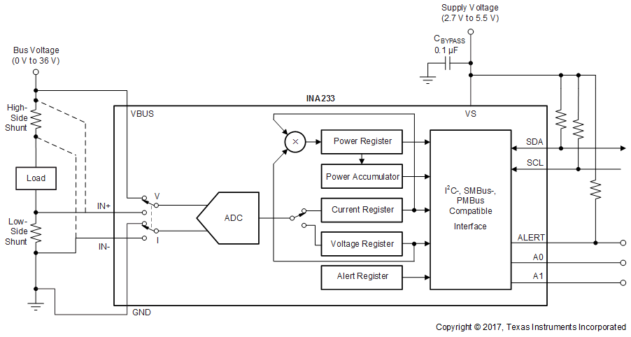
The INA233 device is a current, voltage, and power monitor with an I2C-, SMBus-, and PMBus-compatible interface that is compliant with digital bus voltages from 1.8 V to 5.0 V. The device monitors and reports values for current, voltage, and power. The integrated power accumulator can be used for energy or average power calculations. Programmable calibration value, conversion times, and averaging when combined with an internal multiplier enable direct readouts of current in amperes and power in watts.
The INA233 senses current on common-mode bus voltages that can vary from 0 V to 36 V, independent of the supply voltage. The device operates from a single 2.7-V to 5.5-V supply, drawing a typical supply current of 310 µA in normal operation. The device can be placed in a low-power standby mode where the typical operating current is only 2 µA. The device is specified over the operating temperature range between –40°C and +125°C and features up to 16 programmable addresses.
Device Information(1)
| PART NUMBER | PACKAGE | BODY SIZE (NOM) |
|---|---|---|
| INA233 | VSSOP (10) | 3.00 mm x 3.00 mm |
- For all available packages, see the orderable addendum at the end of the datasheet.
High-Side or Low-Side Sensing Application
