SBOS770A May 2017 – June 2017 INA826S
PRODUCTION DATA.
- 1 Features
- 2 Applications
- 3 Description
- 4 Revision History
- 5 Pin Configuration and Functions
- 6 Specifications
- 7 Detailed Description
- 8 Application and Implementation
- 9 Power Supply Recommendations
- 10Layout
- 11Device and Documentation Support
- 12Mechanical, Packaging, and Orderable Information
Package Options
Mechanical Data (Package|Pins)
- DRC|10
Thermal pad, mechanical data (Package|Pins)
- DRC|10
Orderable Information
10 Layout
10.1 Layout Guidelines
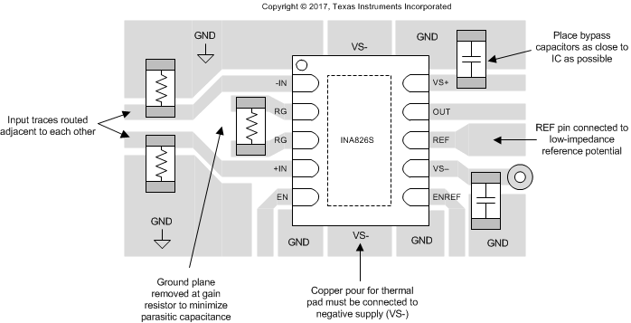
For best operational performance of the device, use good printed circuit board (PCB) layout practices, including:
- Connect low-ESR, 0.1-µF ceramic bypass capacitors between each supply pin and ground, placed as close to the device as possible. A single bypass capacitor from V+ to ground is applicable for single-supply applications. The bypass capacitors are used to reduce the coupled noise by providing low-impedance power sources local to the analog circuitry, because noise can propagate into analog circuitry through the power pins of the circuit as a whole and the op amp specifically.
- Connect the device reference pin to a low-impedance, low-noise, system reference point, such as an analog ground. If a potential other than ground is used as a reference, a low output impedance (such as a voltage divider with an op amp buffer) must be included.
- Minimize the parasitic capacitance and inductance present at the gain resistor connections. Place the gain resistor as close to the device as possible, and remove the ground plane around the gain resistor to minimize parasitic capacitances at these nodes.
- For best performance, route the input traces adjacent to each other as a differential pair.
- For proper amplifier function, connect the package thermal pad to the most negative supply voltage (VEE).
10.2 Layout Example
 Figure 77. INA826S PCB Layout Example