SBOS792A August 2017 – January 2018 INA828
PRODUCTION DATA.
- 1 Features
- 2 Applications
- 3 Description
- 4 Revision History
- 5 Pin Configuration and Functions
- 6 Specifications
- 7 Detailed Description
- 8 Application and Implementation
- 9 Power Supply Recommendations
- 10Layout
- 11Device and Documentation Support
- 12Mechanical, Packaging, and Orderable Information
Package Options
Mechanical Data (Package|Pins)
- D|8
Thermal pad, mechanical data (Package|Pins)
Orderable Information
8.3 PCB Assembly Effects on Precision
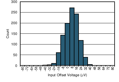
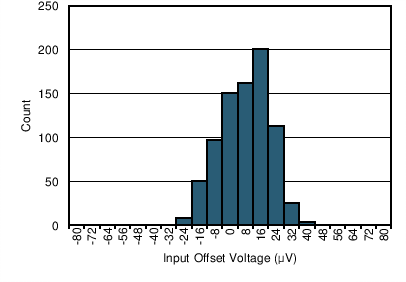
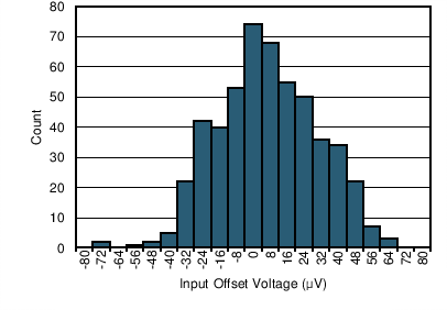
The printed-circuit board (PCB) assembly process, including reflow soldering, imparts thermal stresses on the INA828 which can degrade the precision of the device and must be considered in the development of very-high-precision systems. Baking the PCBs after the assembly process can restore the precision of the device to pre-assembly values. Figure 65, Figure 66, and Figure 67 illustrate the effect of reflow soldering on the typical distribution of input offset voltage of the INA828. Figure 65 shows the distribution of input offset voltage for a set of INA828 devices prior to the PCB assembly process. Exposing the INA828 to a JEDEC-standard thermal profile for reflow soldering produces the histogram shown in Figure 66 on another set of INA828 devices. The standard deviation of input offset voltage has almost doubled due to the thermal stress imparted to the INA828 from the reflow process. However, baking INA828 units for 30 minutes at 125°C after the reflow soldering process produced the distribution given in Figure 67. The post-reflow bake restored the standard deviation of the input offset voltage to pre-assembly levels.
 Figure 65. Typical Distribution of INA828 Input Offset Voltage Prior to Reflow Soldering
 Figure 67. Typical Distribution of Post-Reflow INA828 Units Baked at 125°C for 30 Minutes
 Figure 66. Typical Distribution of INA828 Input Offset Voltage After Reflow Soldering