SBOS792A August 2017 – January 2018 INA828
PRODUCTION DATA.
- 1 Features
- 2 Applications
- 3 Description
- 4 Revision History
- 5 Pin Configuration and Functions
- 6 Specifications
- 7 Detailed Description
- 8 Application and Implementation
- 9 Power Supply Recommendations
- 10Layout
- 11Device and Documentation Support
- 12Mechanical, Packaging, and Orderable Information
Package Options
Mechanical Data (Package|Pins)
- D|8
Thermal pad, mechanical data (Package|Pins)
Orderable Information
7.3.1 Setting the Gain
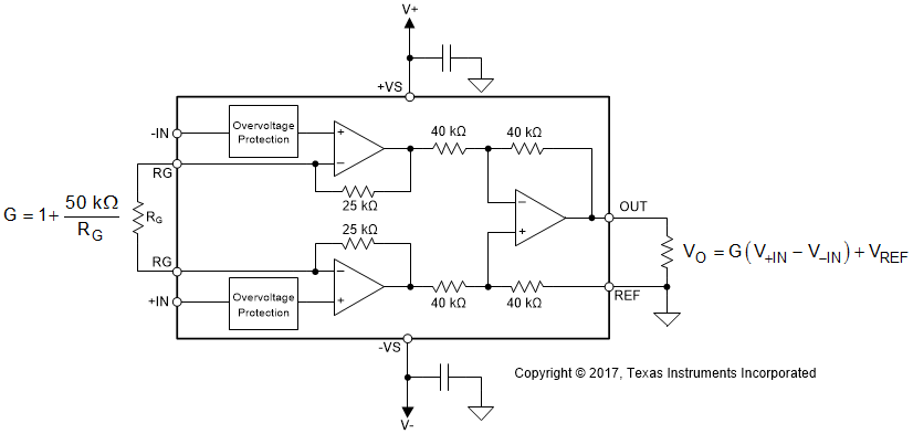
Figure 52 shows that the gain of the INA828 is set by a single external resistor, RG, connected between the RG pins (pins 1 and 8).
 Figure 52. Simplified Diagram of the INA828 With Gain and Output Equations
The value of RG is selected according to:
Equation 1. 

Table 1 lists several commonly-used gains and resistor values. The 50-kΩ term in Equation 1 comes from the sum of the two internal 25-kΩ feedback resistors. These on-chip resistors are laser-trimmed to accurate absolute values. The accuracy and temperature coefficients of these resistors are included in the gain accuracy and drift specifications of the INA828.
Table 1. Commonly-Used Gains and Resistor Values
| DESIRED GAIN | RG (Ω) | NEAREST 1% RG (Ω) |
|---|---|---|
| 1 | NC | NC |
| 2 | 50 k | 49.9 k |
| 5 | 12.5 k | 12.4 k |
| 10 | 5.556 k | 5.49 k |
| 20 | 2.632 k | 2.61 k |
| 50 | 1.02 k | 1.02 k |
| 100 | 505.1 | 511 |
| 200 | 251.3 | 249 |
| 500 | 100.2 | 100 |
| 1000 | 50.05 | 49.9 |