SLLSER4 November 2015 ISO7320-Q1 , ISO7321-Q1
PRODUCTION DATA.
- 1 Features
- 2 Applications
- 3 Description
- 4 Revision History
- 5 Pin Configuration and Functions
-
6 Specifications
- 6.1 Absolute Maximum Ratings
- 6.2 ESD Ratings
- 6.3 Recommended Operating Conditions
- 6.4 Thermal Information
- 6.5 Electrical Characteristics—5-V Supply
- 6.6 Supply Current Characteristics—5-V Supply
- 6.7 Electrical Characteristics—3.3 V
- 6.8 Supply Current Characteristics—3.3-V Supply
- 6.9 Power Dissipation Characteristics
- 6.10 Switching Characteristics—5-V Supply
- 6.11 Switching Characteristics—3.3-V Supply
- 6.12 Typical Characteristics
- 7 Parameter Measurement Information
- 8 Detailed Description
- 9 Application and Implementation
- 10Power Supply Recommendations
- 11Layout
- 12Device and Documentation Support
- 13Mechanical, Packaging, and Orderable Information
Package Options
Refer to the PDF data sheet for device specific package drawings
Mechanical Data (Package|Pins)
- D|8
Thermal pad, mechanical data (Package|Pins)
Orderable Information
1 Features
- Qualified for Automotive Applications
- AEC-Q100 Qualified With the Following Results:
- Device Temperature Grade 1: –40°C to +125°C Ambient Operating Temperature Range
- Device HBM Classification Level 3A
- Device CDM Classification Level C6
- Signaling Rate: 25 Mbps
- Integrated Noise Filter on the Inputs
- Default Output High and Low Options
- Low Power Consumption: Typical ICC per Channel at 1 Mbps:
- ISO7320-Q1: 1.2 mA (5-V Supplies),
0.9 mA (3.3-V Supplies) - ISO7321-Q1: 1.7 mA (5-V Supplies),
1.2 mA (3.3-V Supplies)
- ISO7320-Q1: 1.2 mA (5-V Supplies),
- Low Propagation Delay: 33 ns
Typical (5-V Supplies) - 3.3-V and 5-V Level Translation
- 65-kV/μs Transient Immunity,
Typical (5-V Supplies) - Robust Electromagnetic Compatibility (EMC)
- System-level ESD, EFT, and Surge Immunity
- Low Emissions
- Isolation Barrier Life: > 25 Years
- Operates from 3.3-V and 5-V Supplies
- Narrow Body SOIC-8 Package
- Safety and Regulatory Approvals:
- 4242-VPK Isolation per DIN V VDE V 0884-10 and DIN EN 61010-1
- 3000-VRMS Isolation for 1 minute per UL 1577
- CSA Component Acceptance Notice 5A, IEC 60950-1 and IEC 61010-1 Standards
- Planned CQC Certification per GB4943.1-2011
2 Applications
- Opto-Coupler Replacement in:
- Industrial FieldBus
- ProfiBus
- ModBus
- DeviceNet™ Data Buses
- Servo Control Interface
- Motor Control
- Power Supplies
- Battery Packs
- Industrial FieldBus
3 Description
The ISO732x-Q1 family of devices provides galvanic isolation up to 3000 VRMS for 1 minute per UL 1577 and 4242 VPK per VDE V 0884-10. These devices have two isolated channels comprised of logic input and output buffers separated by silicon dioxide (SiO2) insulation barriers.
The ISO7320-Q1 has both channels in the same direction while ISO7321-Q1 has the two channels in opposite direction. In case of input power or signal loss, the default output is low for orderable part numbers with suffix F and high for orderable part numbers without suffix F. See Device Functional Modes for more information. Used in conjunction with isolated power supplies, these devices prevent noise currents on a data bus or other circuits from entering the local ground and interfering with or damaging sensitive circuitry. The ISO732x-Q1 family of devices has integrated noise filters for harsh industrial environment where short noise pulses may be present at the device input pins. The ISO732x-Q1 family of devices has TTL input thresholds and operate from 3-V to 5.5-V supply levels.
Through innovative chip design and layout techniques, electromagnetic compatibility of the ISO732x-Q1 family of devices has been significantly enhanced to enable system-level ESD, EFT, Surge and Emissions compliance.
Device Information(1)
| PART NUMBER | PACKAGE | BODY SIZE (NOM) |
|---|---|---|
| ISO7320-Q1 | SOIC (8) | 4.90 mm × 3.91 mm |
| ISO7321-Q1 |
- For all available packages, see the orderable addendum at the end of the datasheet.
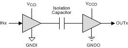
Simplified Schematic

4 Revision History
| DATE | REVISION | NOTES |
|---|---|---|
| November 2015 | * | Initial release. |