SLLS984I June 2009 – July 2015 ISO7420 , ISO7420M , ISO7421
UNLESS OTHERWISE NOTED, this document contains PRODUCTION DATA.
- 1 Features
- 2 Applications
- 3 Description
- 4 Revision History
- 5 Pin Configuration and Functions
-
6 Specifications
- 6.1 Absolute Maximum Ratings
- 6.2 ESD Ratings
- 6.3 Recommended Operating Conditions
- 6.4 Thermal Information
- 6.5 Electrical Characteristics: VCC1 and VCC2 at 5 V ±5%
- 6.6 Electrical Characteristics: VCC1 at 5 V ±5%, VCC2 at 3.3 V ±5%
- 6.7 Electrical Characteristics: VCC1 at 3.3 V ±5%, VCC2 at 5 V ±5%
- 6.8 Electrical Characteristics: VCC1 and VCC2 at 3.3 V ±5%
- 6.9 Power Dissipation Characteristics
- 6.10 Switching Characteristics: VCC1 and VCC2 at 5 V ±5%
- 6.11 Switching Characteristics: VCC1 at 5 V ±5%, VCC2 at 3.3 V ±5%
- 6.12 Switching Characteristics: VCC1 at 3.3 V ±5%, VCC2 at 5 V ±5%
- 6.13 Switching Characteristics: VCC1 and VCC2 at 3.3 V ±5%
- 6.14 Typical Characteristics
- 7 Parameter Measurement Information
- 8 Detailed Description
- 9 Application and Implementation
- 10Power Supply Recommendations
- 11Layout
- 12Device and Documentation Support
- 13Mechanical, Packaging, and Orderable Information
Package Options
Mechanical Data (Package|Pins)
- D|8
Thermal pad, mechanical data (Package|Pins)
Orderable Information
1 Features
- Highest Signaling Rate: 1 Mbps
- Low Power Consumption, Typical ICC per Channel (3.3-V operation):
- ISO7420: 1.1 mA, ISO7421: 1.5 mA
- Low Propagation Delay – 9 ns Typical
- Low Skew – 300 ps Typical
- Wide TA Range: –40°C to 125°C (M-Grade)
- 50-kV/μs Transient Immunity, Typical
- Over 25-Year Isolation Integrity at Rated Voltage
- Operates From 3.3-V and 5-V Supply and Logic Levels
- 3.3-V and 5-V Level Translation
- Narrow Body SOIC-8 Package
- Safety and Regulatory Approvals:
- 4242 VPK Isolation per DIN V VDE V 0884-10 and DIN EN 61010-1
- 2500 VRMS Isolation for 1 minute per UL 1577
- CSA Component Acceptance Notice 5A, IEC 60950-1 and IEC 61010-1 Standards
- CQC Certification per GB4943.1-2011
2 Applications
- Optocoupler Replacement in:
- Industrial Fieldbus
- Profibus
- Modbus
- DeviceNet™ Data Buses
- Servo Control Interface
- Motor Control
- Power Supplies
- Battery Packs
- Industrial Fieldbus
3 Description
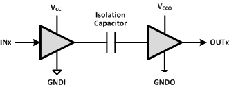
The ISO7420, ISO7420M and ISO7421 provide galvanic isolation up to 2500 VRMS for 1 minute per UL. These digital isolators have two isolated channels. Each isolation channel has a logic input and output buffer separated by a silicon dioxide (SiO2) insulation barrier. Used in conjunction with isolated power supplies, these devices prevent noise currents on a data bus or other circuit from entering the local ground and interfering with or damaging sensitive circuitry. The suffix M indicates wide temperature range (–40°C to 125°C).
These devices have TTL input thresholds and require two supply voltages, 3.3 or 5 V, or any combination. All inputs are 5-V tolerant when supplied from a 3.3-V supply.
Note: The ISO7420 and ISO7421 are specified for signaling rates up to 1 Mbps. Due to their fast response time, under most cases, these devices will also transmit data with much shorter pulse widths. Designers should add external filtering to remove spurious signals with input pulse duration <20 ns if desired.
Device Information(1)
| PART NUMBER | PACKAGE | BODY SIZE (NOM) |
|---|---|---|
| ISO7420 | SOIC (8) | 4.90 mm × 3.91 mm |
| ISO7420M | ||
| ISO7421 |
- For all available packages, see the orderable addendum at the end of the data sheet.
Simplified Schematic
