SNOSD55 June 2017 LF356-MIL
PRODUCTION DATA.
- 1 Features
- 2 Applications
- 3 Description
- 4 Revision History
- 5 Pin Configuration and Functions
-
6 Specifications
- 6.1 Absolute Maximum Ratings
- 6.2 ESD Ratings
- 6.3 Recommended Operating Conditions
- 6.4 Thermal Information
- 6.5 AC Electrical Characteristics, TA = TJ = 25°C, VS = ±15 V
- 6.6 DC Electrical Characteristics, TA = TJ = 25°C, VS = ±15 V
- 6.7 DC Electrical Characteristics
- 6.8 Power Dissipation Ratings
- 6.9 Typical Characteristics
- 7 Detailed Description
- 8 Application and Implementation
- 9 Power Supply Recommendations
- 10Layout
- 11Device and Documentation Support
- 12Mechanical, Packaging, and Orderable Information
Package Options
Mechanical Data (Package|Pins)
- YS|0
- LMC|8
Thermal pad, mechanical data (Package|Pins)
Orderable Information
1 Features
- Advantages
- Replace Expensive Hybrid and Module FET Op Amps
- Rugged JFETs Allow Blow-Out Free Handling Compared With MOSFET Input Devices
- Excellent for Low Noise Applications Using Either High or Low Source Impedance—Very Low 1/f Corner
- Offset Adjust Does Not Degrade Drift or Common-Mode Rejection as in Most Monolithic Amplifiers
- New Output Stage Allows Use of Large Capacitive Loads (5,000 pF) Without Stability Problems
- Internal Compensation and Large Differential Input Voltage Capability
- Common Features
- Low Input Bias Current: 30 pA
- Low Input Offset Current: 3 pA
- High Input Impedance: 1012 Ω
- Low Input Noise Current: 0.01 pA/√Hz
- High Common-Mode Rejection Ratio: 100 dB
- Large DC Voltage Gain: 106 dB
- Uncommon Features
- Extremely Fast Settling Time to 0.01%: 1.5 μs
- Fast Slew Rate: 12 V/µs
- Wide Gain Bandwidth: 5 MHz
- Low Input Noise Voltage: 12 nV/√Hz
2 Applications
- Precision High-Speed Integrators
- Fast D/A and A/D Converters
- High Impedance Buffers
- Wideband, Low Noise, Low Drift Amplifiers
- Logarithmic Amplifiers
- Photocell Amplifiers
- Sample and Hold Circuits
3 Description
The LF356-MIL device are the first monolithic JFET input operational amplifiers to incorporate well-matched, high-voltage JFETs on the same chip with standard bipolar transistors (BI-FET™ Technology). These amplifiers feature low input bias and offset currents/low offset voltage and offset voltage drift, coupled with offset adjust, which does not degrade drift or common-mode rejection. The devices are also designed for high slew rate, wide bandwidth, extremely fast settling time, low voltage and current noise and a low 1/f noise corner.
Device Information(1)
| PART NUMBER | PACKAGE | BODY SIZE (NOM) |
|---|---|---|
| LF356-MIL | SOIC (8) | 4.90 mm × 3.91 mm |
| TO-CAN (8) | 9.08 mm × 9.08 mm | |
| PDIP (8) | 9.81 mm × 6.35 mm |
- For all available packages, see the orderable addendum at the end of the data sheet.
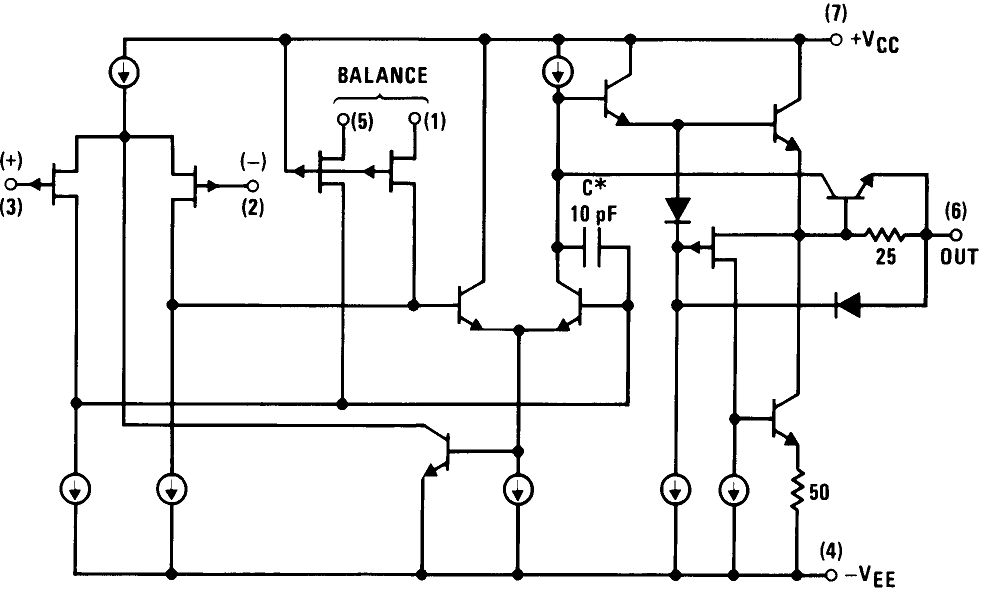
Simplified Schematic

3 pF in LF357 series
4 Revision History
| DATE | REVISION | NOTES |
|---|---|---|
| June 2017 | * | Initial release. |