SNVS038H July 1999 – January 2015 LM1085
PRODUCTION DATA.
- 1 Features
- 2 Applications
- 3 Description
- 4 Revision History
- 5 Pin Configuration and Functions
- 6 Specifications
- 7 Detailed Description
-
8 Application and Implementation
- 8.1 Application Information
- 8.2
Typical Applications
- 8.2.1 1.2-V to 15-V Adjustable Regulator
- 8.2.2 Adjustable at 5 V
- 8.2.3 5-V Regulator with Shutdown
- 8.2.4 Battery Charger
- 8.2.5 Adjustable Fixed Regulator
- 8.2.6 Regulator with Reference
- 8.2.7 High Current Lamp Driver Protection
- 8.2.8 Battery Backup Regulated Supply
- 8.2.9 Ripple Rejection Enhancement
- 8.2.10 Automatic Light Control
- 8.2.11 Generating Negative Supply Voltage
- 8.2.12 Remote Sensing
- 9 Power Supply Recommendations
- 10Layout
- 11Device and Documentation Support
- 12Mechanical, Packaging, and Orderable Information
Package Options
Mechanical Data (Package|Pins)
Thermal pad, mechanical data (Package|Pins)
- KTT|3
Orderable Information
10 Layout
10.1 Layout Guidelines
For the best overall performance, some layout guidelines should be followed. Place all circuit components on the same side of the circuit board and as near as practical to the respective linear regulator pins connections. Traces should be kept short and wide to reduce the amount of parasitic elements into the system. The actual width and thickness of traces will depend on the current carrying capability and heat dissipation required by the end system. An array of plated vias can be placed on the pad area underneath the TAB to conduct heat to any inner plane areas or to a bottom-side copper plane.
10.2 Layout Example
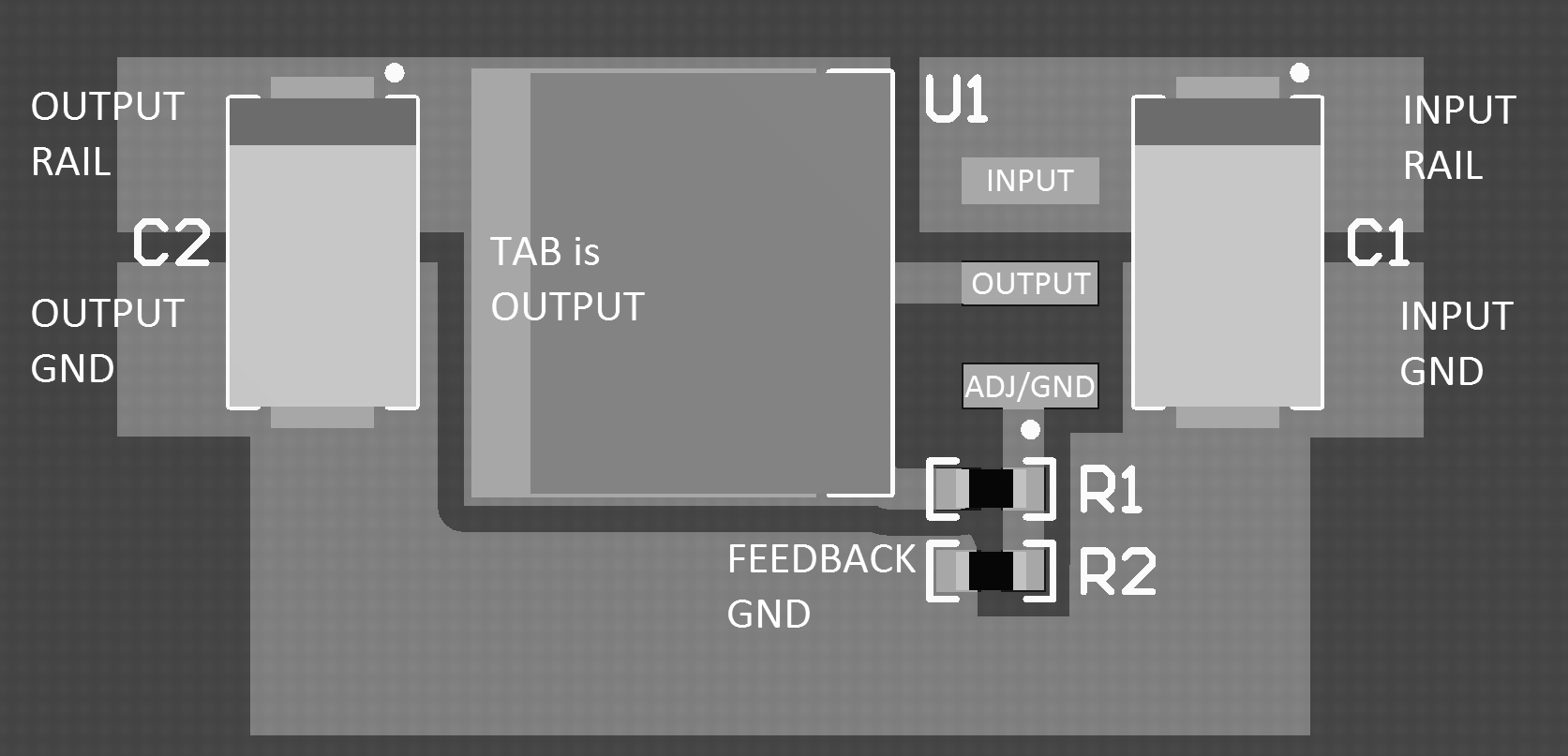 Figure 27. Layout Example
10.3 Thermal Considerations
ICs heats up when in operation, and power consumption is one factor in how hot it gets. The other factor is how well the heat is dissipated. Heat dissipation is predictable by knowing the thermal resistance between the IC and ambient (θJA). Thermal resistance has units of temperature per power (C/W). The higher the thermal resistance, the hotter the IC.
The LM1085 specifies the thermal resistance for each package as junction to case (θJC). In order to get the total resistance to ambient (θJA), two other thermal resistance must be added, one for case to heat-sink (θCH) and one for heatsink to ambient (θHA). The junction temperature can be predicted as follows:
TJ is junction temperature, TA is ambient temperature, and PD is the power consumption of the device. Device power consumption is calculated as follows:
Figure 28 shows the voltages and currents which are present in the circuit.
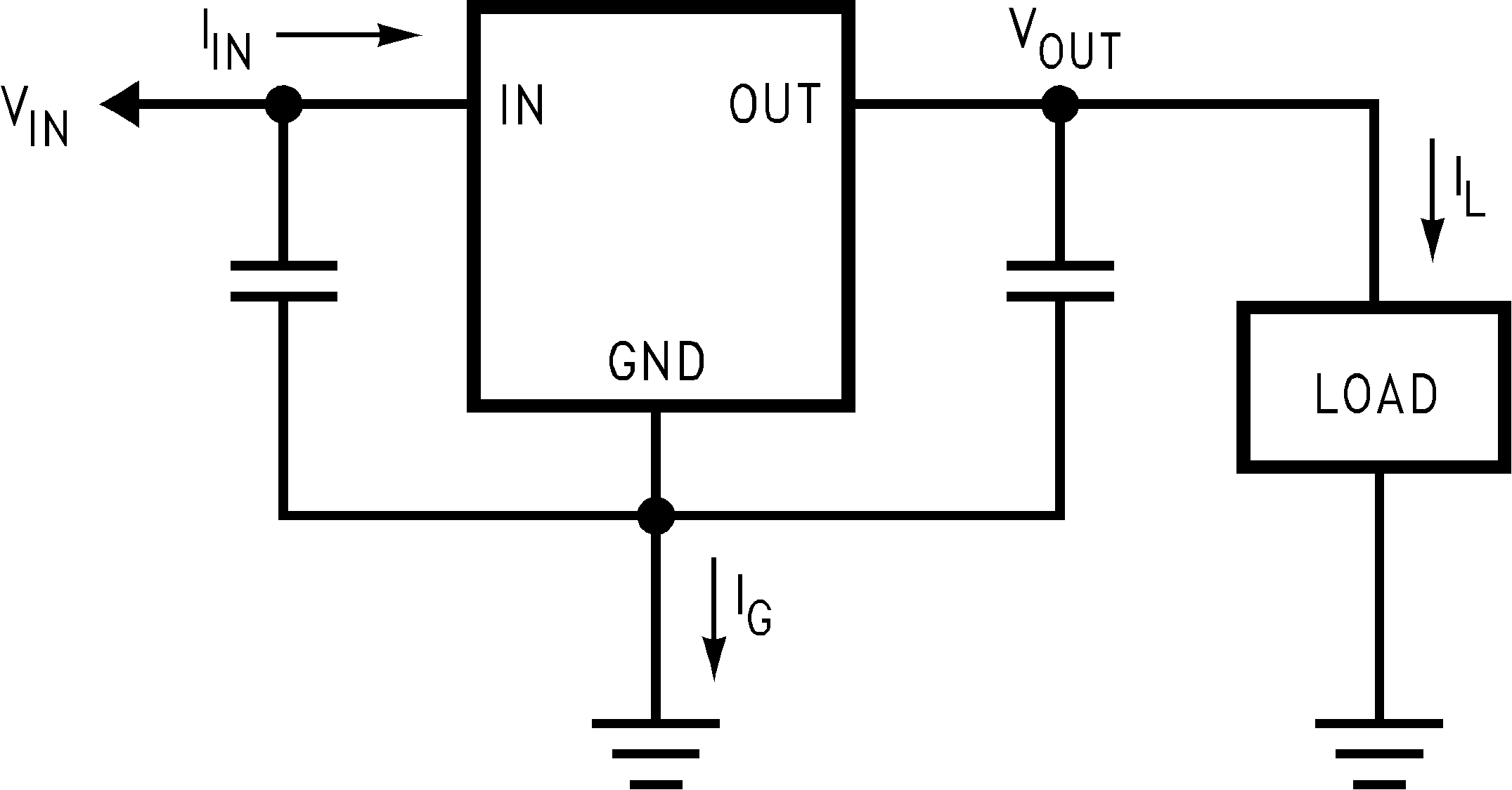 Figure 28. Power Dissipation Diagram
Once the devices power is determined, the maximum allowable (θJA (max)) is calculated as:
θJA (max) = TR(max)/PD = TJ(max) − TA(max)/PD
The LM1085 has different temperature specifications for two different sections of the IC: the control section and the output section. The Thermal Information table shows the junction to case thermal resistances for each of these sections, while the maximum junction temperatures (TJ(max)) for each section is listed in the Absolute Maximum Ratings section of the datasheet. TJ(max) is 125°C for the control section, while TJ(max) is 150°C for the output section.
θJA (max) should be calculated separately for each section as follows:
The required heat sink is determined by calculating its required thermal resistance (θHA (max)).
(θHA (max)) should also be calculated twice as follows:
If thermal compound is used, θCH can be estimated at 0.2 C/W. If the case is soldered to the heat sink, then a θCH can be estimated as 0 C/W.
After, θHA (max) is calculated for each section, choose the lower of the two θHA (max) values to determine the appropriate heat sink.
If PC board copper is going to be used as a heat sink, then Figure 29 can be used to determine the appropriate area (size) of copper foil required.
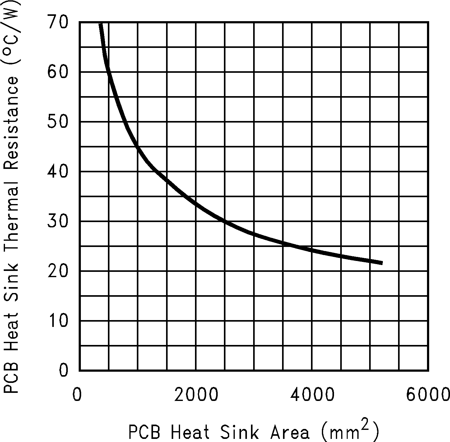 Figure 29. Heat Sink Thermal Resistance vs Area