SNVS038H July 1999 – January 2015 LM1085
PRODUCTION DATA.
- 1 Features
- 2 Applications
- 3 Description
- 4 Revision History
- 5 Pin Configuration and Functions
- 6 Specifications
- 7 Detailed Description
-
8 Application and Implementation
- 8.1 Application Information
- 8.2
Typical Applications
- 8.2.1 1.2-V to 15-V Adjustable Regulator
- 8.2.2 Adjustable at 5 V
- 8.2.3 5-V Regulator with Shutdown
- 8.2.4 Battery Charger
- 8.2.5 Adjustable Fixed Regulator
- 8.2.6 Regulator with Reference
- 8.2.7 High Current Lamp Driver Protection
- 8.2.8 Battery Backup Regulated Supply
- 8.2.9 Ripple Rejection Enhancement
- 8.2.10 Automatic Light Control
- 8.2.11 Generating Negative Supply Voltage
- 8.2.12 Remote Sensing
- 9 Power Supply Recommendations
- 10Layout
- 11Device and Documentation Support
- 12Mechanical, Packaging, and Orderable Information
Package Options
Mechanical Data (Package|Pins)
Thermal pad, mechanical data (Package|Pins)
Orderable Information
6 Specifications
6.1 Absolute Maximum Ratings
over operating free-air temperature range (unless otherwise noted) (1)(2)| MIN | MAX | UNIT | |||
|---|---|---|---|---|---|
| Maximum Input to Output Voltage Differential | |||||
| LM1085-ADJ | 29 | V | |||
| LM1085-12 | 18 | V | |||
| LM1085-3.3 | 27 | V | |||
| LM1085-5.0 | 25 | V | |||
| Power Dissipation (1) | Internally Limited | V | |||
| Junction Temperature (TJ)(2) | 150 | °C | |||
| Lead Temperature | 260, to 10 sec | °C | |||
| Storage temperature range, Tstg | –65 | 150 | °C | ||
(1) Stresses beyond those listed under Absolute Maximum Ratings may cause permanent damage to the device. These are stress ratings only, which do not imply functional operation of the device at these or any other conditions beyond those indicated under Recommended Operating Conditions. Exposure to absolute-maximum-rated conditions for extended periods may affect device reliability.
6.2 ESD Ratings
| VALUE | UNIT | |||
|---|---|---|---|---|
| V(ESD) | Electrostatic discharge | Human-body model (HBM), per ANSI/ESDA/JEDEC JS-001(1) | ±2000 | V |
(1) JEDEC document JEP155 states that 500-V HBM allows safe manufacturing with a standard ESD control process.
6.3 Recommended Operating Conditions
over operating free-air temperature range (unless otherwise noted)| MIN | MAX | UNIT | ||
|---|---|---|---|---|
| Junction Temperature (TJ)(2) | −40 | 125 | °C | |
6.4 Thermal Information
| THERMAL METRIC(1) | LM1085 | UNIT | ||
|---|---|---|---|---|
| KTT | NDE | |||
| 3 PINS | 3 PINS | |||
| RθJA | Junction-to-ambient thermal resistance | 40.6 | 22.8 | °C/W |
| RθJC(top) | Junction-to-case (top) thermal resistance | 43.0 | 15.6 | |
| RθJB | Junction-to-board thermal resistance | 23.1 | 4.2 | |
| ψJT | Junction-to-top characterization parameter | 9.9 | 2.2 | |
| ψJB | Junction-to-board characterization parameter | 22.1 | 4.2 | |
| RθJC(bot) | Junction-to-case (bottom) thermal resistance | 0.7 | 0.7 | |
(1) For more information about traditional and new thermal metrics, see the IC Package Thermal Metrics application report, SPRA953.
6.5 Electrical Characteristics
Minimum and Maximum limits are ensured through test, design, or statistical correlation. Typical values represent the most likely parametric norm at TJ = 25°C, and are provided for reference purposes only.| PARAMETER | TEST CONDITIONS | MIN(4) | TYP(3) | MAX(4) | UNIT | |
|---|---|---|---|---|---|---|
| VREF | Reference Voltage (5) |
LM1085-ADJ, IOUT = 10 mA, VIN − VOUT = 3 V, 10 mA ≤ IOUT ≤ IFULL LOAD,1.5 V ≤ (VIN−VOUT) ≤ 15 V | 1.238 | 1.250 | 1.262 | V |
| LM1085-ADJ, IOUT = 10 mA, VIN − VOUT = 3 V, 10 mA ≤ IOUT ≤ IFULL LOAD,1.5 V ≤ (VIN − VOUT) ≤ 15 V, –40°C ≤ TJ ≤ 125°C | 1.225 | 1.250 | 1.270 | |||
| VOUT | Output Voltage (5) |
LM1085-3.3, IOUT = 0 mA, VIN = 5 V, 0 ≤ IOUT ≤ IFULL LOAD, 4.8 V ≤ VIN ≤ 15 V | 3.270 | 3.300 | 3.330 | V |
| LM1085-3.3, IOUT = 0 mA, VIN = 5 V, 0 ≤ IOUT ≤ IFULL LOAD, 4.8 V ≤ VIN ≤ 15 V, –40°C ≤ TJ ≤ 125°C | 3.235 | 3.300 | 3.365 | |||
| LM1085-5.0, IOUT = 0 mA, VIN = 8 V, 0 ≤ IOUT ≤ IFULL LOAD, 6.5 V ≤ VIN ≤ 20 V | 4.950 | 5.000 | 5.050 | V | ||
| LM1085-5.0, IOUT = 0 mA, VIN = 8 V, 0 ≤ IOUT ≤ IFULL LOAD, 6.5 V ≤ VIN ≤ 20 V, –40°C ≤ TJ ≤ 125°C | 4.900 | 5.000 | 5.100 | |||
| LM1085-12, IOUT = 0 mA, VIN = 15 V, 0 ≤ IOUT ≤ IFULL LOAD, 13.5 V ≤ VIN ≤ 25 V | 11.880 | 12.000 | 12.120 | V | ||
| LM1085-12, IOUT = 0 mA, VIN = 15 V, 0 ≤ IOUT ≤ IFULL LOAD, 13.5 V ≤ VIN ≤ 25 V, –40°C ≤ TJ ≤ 125°C | 11.760 | 12.000 | 12.240 | |||
| ΔVOUT | Line Regulation (6) |
LM1085-ADJ, IOUT =10 mA, 1.5 V ≤ (VIN-VOUT) ≤ 15 V | 0.015 | 0.2 | ||
| LM1085-ADJ, IOUT =10 mA, 1.5 V ≤ (VIN-VOUT) ≤ 15 V, –40°C ≤ TJ ≤ 125°C | 0.035 | 0.2 | ||||
| LM1085-3.3, IOUT = 0 mA, 4.8 V ≤ VIN ≤ 15 V | 0.5 | 6 | mV | |||
| LM1085-3.3, IOUT = 0 mA, 4.8 V ≤ VIN ≤ 15 V, –40°C ≤ TJ ≤ 125°C | 1.0 | 6 | ||||
| LM1085-5.0, IOUT = 0 mA, 6.5 V ≤ VIN ≤ 20 V | 0.5 | 10 | mV | |||
| LM1085-5.0, IOUT = 0 mA, 6.5 V ≤ VIN ≤ 20 V, –40°C ≤ TJ ≤ 125°C | 1.0 | 10 | ||||
| LM1085-12, I OUT = 0 mA, 13.5 V ≤ VIN ≤ 25 V | 1.0 | 25 | mV | |||
| LM1085-12, I OUT = 0 mA, 13.5 V ≤ VIN ≤ 25 V, –40°C ≤ TJ ≤ 125°C | 2.0 | 25 | ||||
| ΔVOUT | Load Regulation (6) |
LM1085-ADJ, (VIN-V OUT) = 3 V, 10 mA ≤ IOUT ≤ IFULL LOAD | 0.1 | 0.3 | ||
| LM1085-ADJ, (VIN-V OUT) = 3 V, 10 mA ≤ IOUT ≤ IFULL LOAD, –40°C ≤ TJ ≤ 125°C | 0.2 | 0.4 | ||||
| LM1085-3.3, VIN = 5 V, 0 ≤ IOUT ≤ IFULL LOAD | 3 | 15 | mV | |||
| LM1085-3.3, VIN = 5 V, 0 ≤ IOUT ≤ IFULL LOAD, –40°C ≤ TJ ≤ 125°C | 7 | 20 | ||||
| LM1085-5.0, VIN = 8 V, 0 ≤ IOUT ≤ IFULL LOAD | 5 | 20 | mV | |||
| LM1085-5.0, VIN = 8 V, 0 ≤ IOUT ≤ IFULL LOAD, –40°C ≤ TJ ≤ 125°C | 10 | 35 | ||||
| LM1085-12, VIN = 15 V, 0 ≤ IOUT ≤ IFULL LOAD | 12 | 36 | mV | |||
| LM1085-12, VIN = 15 V, 0 ≤ IOUT ≤ IFULL LOAD, –40°C ≤ TJ ≤ 125°C | 24 | 72 | ||||
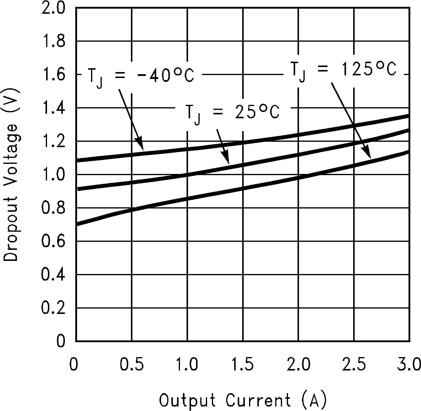
| VDO | Dropout Voltage (7) | LM1085-ADJ, 3.3, 5, 12, ΔVREF, ΔVOUT = 1%, IOUT = 3A, –40°C ≤ TJ ≤ 125°C | 1.3 | 1.5 | V | |
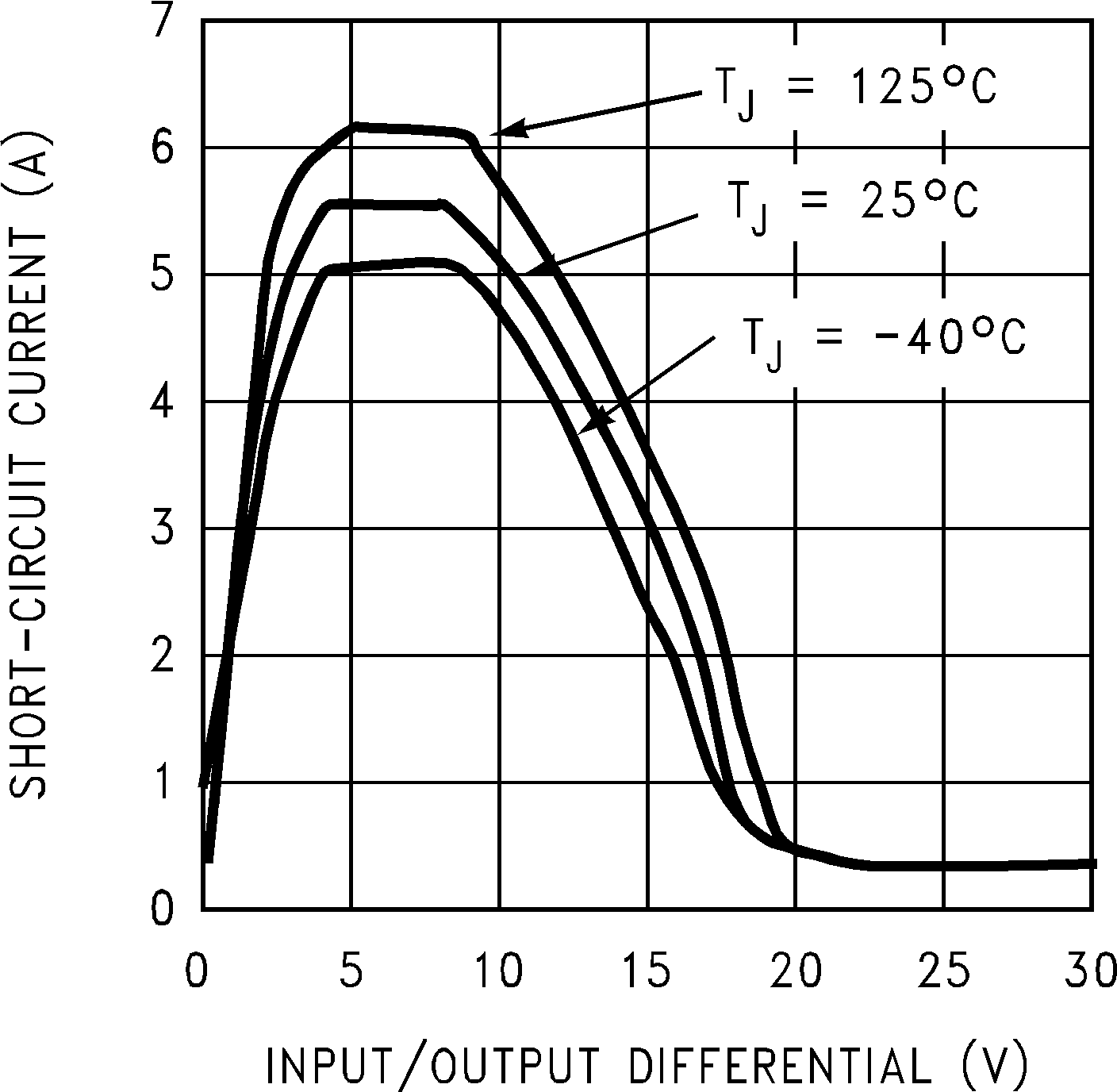
| ILIMIT | Current Limit | LM1085-ADJ, VIN−VOUT = 5 V, –40°C ≤ TJ ≤ 125°C | 3.2 | 5.5 | A | |
| LM1085-ADJ, VIN−VOUT = 25 V, –40°C ≤ TJ ≤ 125°C | 0.2 | 0.5 | ||||
| LM1085-3.3, VIN = 8.0 V, –40°C ≤ TJ ≤ 125°C | 3.2 | 5.5 | A | |||
| LM1085-5.0, VIN = 10 V, –40°C ≤ TJ ≤ 125°C | 3.2 | 5.5 | A | |||
| LM1085-12, VIN = 17 V, –40°C ≤ TJ ≤ 125°C | 3.2 | 5.5 | A | |||
| Minimum Load Current (8) | LM1085-ADJ, VIN −VOUT = 25 V, –40°C ≤ TJ ≤ 125°C | 5.0 | 10.0 | mA | ||
| IGND | Quiescent Current | LM1085-3.3, VIN ≤ 18 V, –40°C ≤ TJ ≤ 125°C | 5.0 | 10.0 | mA | |
| LM1085-5.0, VIN ≤ 20 V, –40°C ≤ TJ ≤ 125°C | 5.0 | 10.0 | mA | |||
| LM1085-12, VIN ≤ 25 V, –40°C ≤ TJ ≤ 125°C | 5.0 | 10.0 | mA | |||
| Thermal Regulation | TA = 25°C, 30ms Pulse | .004 | 0.02 | %/W | ||
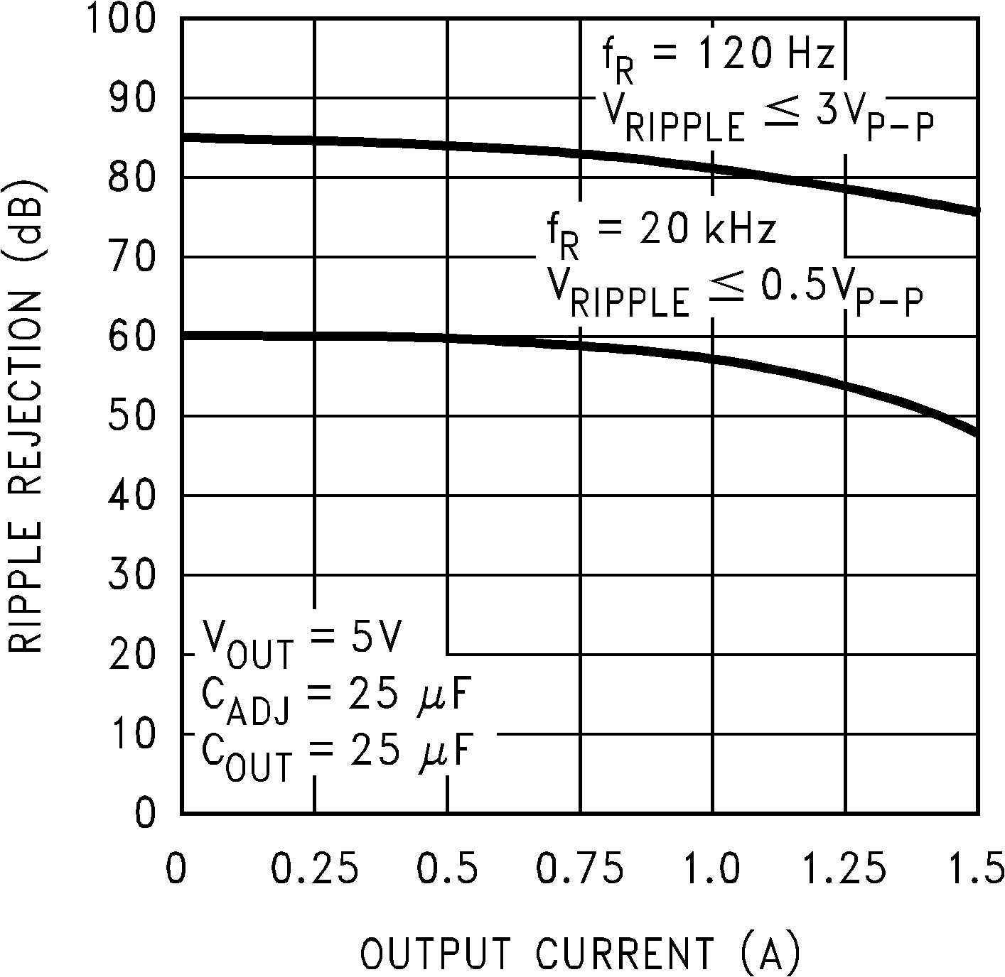
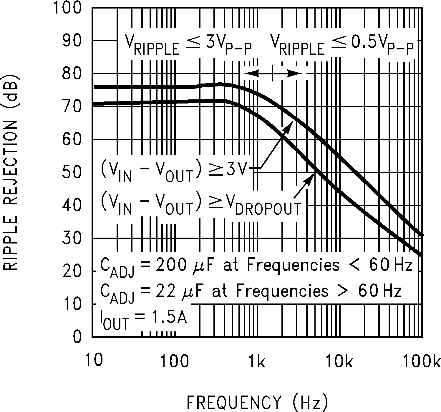
| Ripple Rejection | fRIPPLE = 120Hz, COUT = 25µF Tantalum, IOUT = 3A, LM1085-ADJ, CADJ = 25µF, (VIN−VO) = 3 V, –40°C ≤ TJ ≤ 125°C | 60 | 75 | dB | ||
| LM1085-3.3, VIN = 6.3 V, –40°C ≤ TJ ≤ 125°C | 60 | 72 | dB | |||
| LM1085-5.0, VIN = 8.0 V, –40°C ≤ TJ ≤ 125°C | 60 | 68 | dB | |||
| LM1085-12, VIN = 15 V, –40°C ≤ TJ ≤ 125°C | 54 | 60 | dB | |||
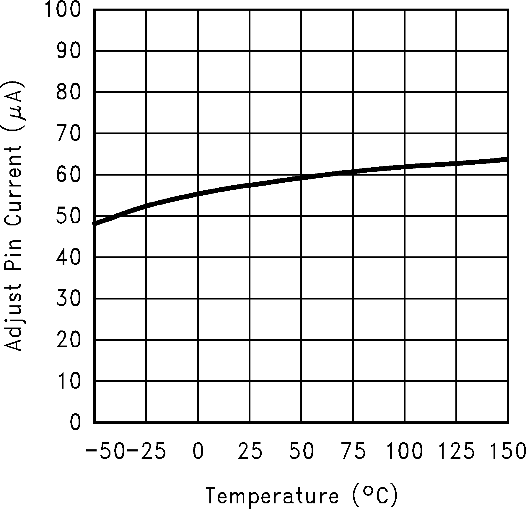
| IADJ | Adjust Pin Current | LM1085–ADJ | 55 | µA | ||
| LM1085–ADJ, –40°C ≤ TJ ≤ 125°C | 120 | |||||
| ΔIADJ | Adjust Pin Current Change | LM1085–ADJ, 10mA ≤ IOUT ≤ IFULL LOAD, 1.5 V ≤ VIN−VOUT ≤ 25 V, –40°C ≤ TJ ≤ 125°C | 0.2 | 5 | µA | |
| Temperature Stability | –40°C ≤ TJ ≤ 125°C | 0.5 | ||||
| Long Term Stability | TA= 125°C, 1000 Hrs | 0.3 | 1.0 | |||
| RMS Output Noise (% of VOUT) | 10Hz ≤ f ≤ 10 kHz | 0.003 | ||||
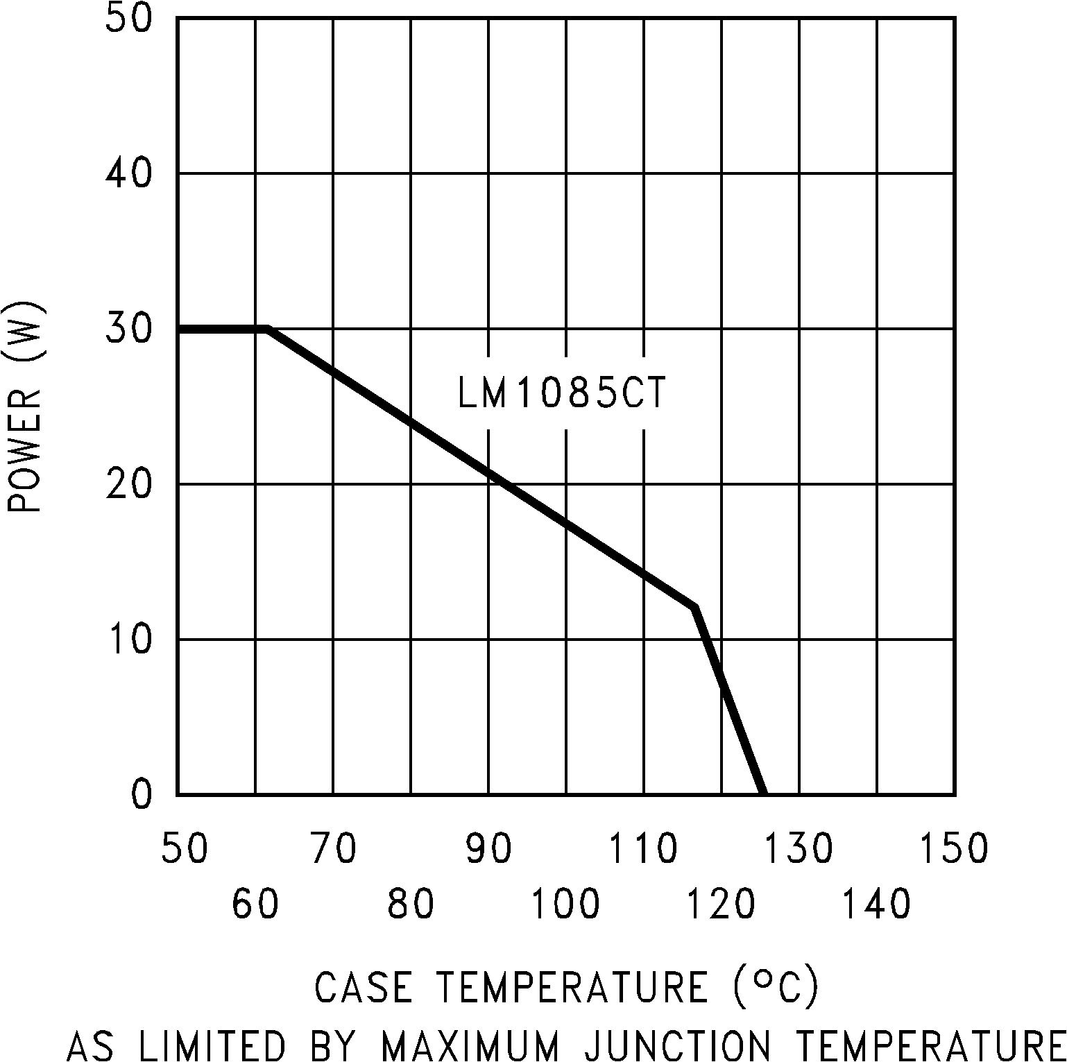
(1) Power dissipation is kept in a safe range by current limiting circuitry. Refer to Overload Recovery.
(2) The maximum power dissipation is a function of TJ(max) , θJA, and TA. The maximum allowable power dissipation at any ambient temperature is PD = (TJ(max)–T A)/θJA. All numbers apply for packages soldered directly into a PC board. Refer to Thermal Considerations in the Application Notes.
(3) Typical Values represent the most likely parametric norm.
(4) All limits are specified by testing or statistical analysis.
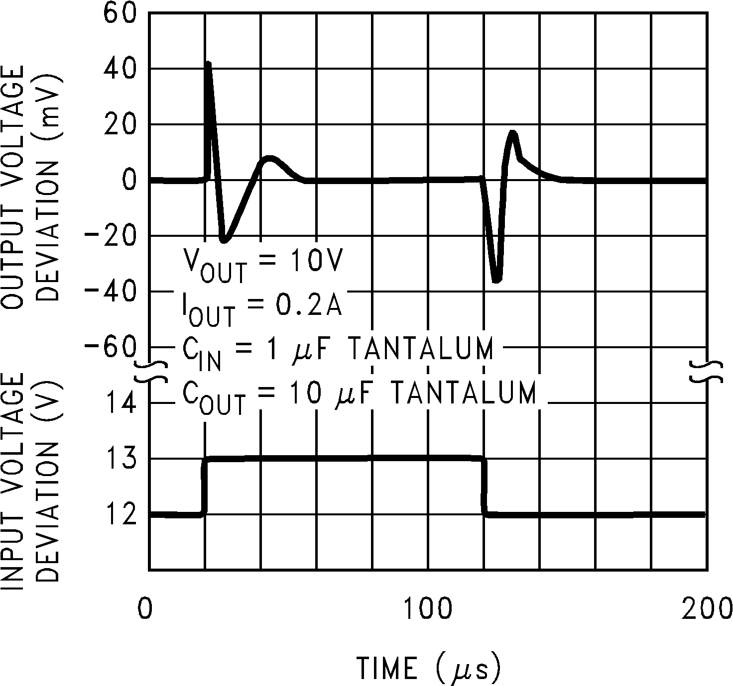
(5) IFULL LOAD is defined in the current limit curves. The IFULL LOAD Curve defines the current limit as a function of input-to-output voltage. Note that 30W power dissipation for the LM1085 is only achievable over a limited range of input-to-output voltage.
(6) Load and line regulation are measured at constant junction temperature, and are ensured up to the maximum power dissipation of 30W. Power dissipation is determined by the input/output differential and the output current. Ensured maximum power dissipation will not be available over the full input/output range.
(7) Dropout voltage is specified over the full output current range of the device.
(8) The minimum output current required to maintain regulation.
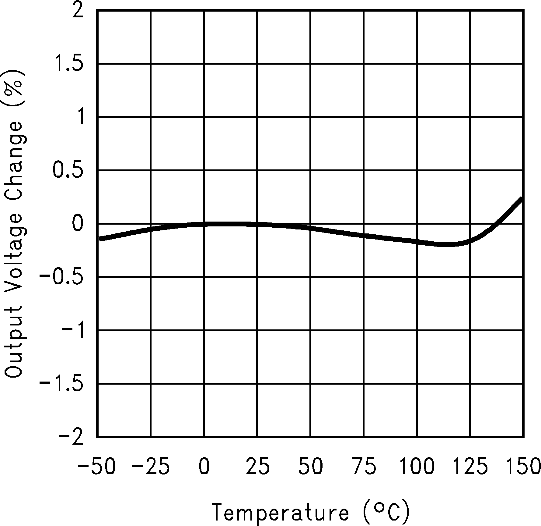
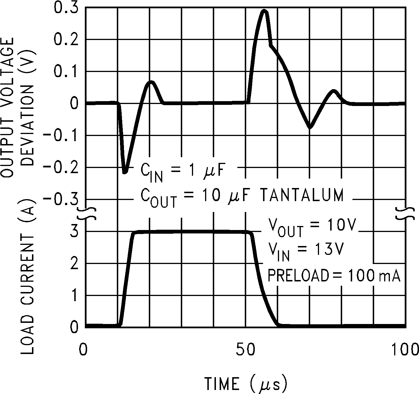
6.6 Typical Characteristics