SNVS483H January   2007  – August 2017 LM25574

PRODUCTION DATA.  

  1. Features
  2. Applications
  3. Description
    1.     Device Images
      1.      Simplified Application Schematic
  4. Revision History
  5. Pin Configuration and Functions
    1.     Pin Functions
  6. Specifications
    1. 6.1 Absolute Maximum Ratings
    2. 6.2 ESD Ratings
    3. 6.3 Recommended Operating Conditions
    4. 6.4 Thermal Information
    5. 6.5 Electrical Characteristics
    6. 6.6 Typical Characteristics
  7. Detailed Description
    1. 7.1 Overview
    2. 7.2 Functional Block Diagram
    3. 7.3 Feature Description
      1. 7.3.1 High Voltage Start-Up Regulator
    4. 7.4 Device Functional Modes
      1. 7.4.1 Shutdown and Stand-by Mode
      2. 7.4.2 Oscillator and Sync Capability
      3. 7.4.3 Error Amplifier and PWM Comparator
      4. 7.4.4 Ramp Generator
      5. 7.4.5 Maximum Duty Cycle and Input Drop-out Voltage
      6. 7.4.6 Current Limit
      7. 7.4.7 Soft-Start
      8. 7.4.8 Boost Pin
      9. 7.4.9 Thermal Protection
  8. Application and Implementation
    1. 8.1 Application Information
      1. 8.1.1  External Components
      2. 8.1.2  R3 (RT)
      3. 8.1.3  L1
      4. 8.1.4  C3 (CRAMP)
      5. 8.1.5  C9
      6. 8.1.6  C1
      7. 8.1.7  C8
      8. 8.1.8  C7
      9. 8.1.9  C4
      10. 8.1.10 R5, R6
      11. 8.1.11 R1, R2, C2
      12. 8.1.12 R4, C5, C6
      13. 8.1.13 Bias Power Dissipation Reduction
    2. 8.2 Typical Application
      1. 8.2.1 Typical Schematic for High Frequency (1MHz) Application
      2. 8.2.2 Detailed Design Procedure
        1. 8.2.2.1 Custom Design With WEBENCH® Tools
  9. Layout
    1. 9.1 Layout Guidelines
      1. 9.1.1 PCB Layout and Thermal Considerations
    2. 9.2 Layout Example
  10. 10Device and Documentation Support
    1. 10.1 Device Support
      1. 10.1.1 Developmental Support
        1. 10.1.1.1 Custom Design With WEBENCH® Tools
    2. 10.2 Receiving Notification of Documentation Updates
    3. 10.3 Community Resources
    4. 10.4 Trademarks
    5. 10.5 Electrostatic Discharge Caution
    6. 10.6 Glossary
  11. 11Mechanical, Packaging, and Orderable Information

Package Options

Mechanical Data (Package|Pins)
Thermal pad, mechanical data (Package|Pins)
Orderable Information

Bias Power Dissipation Reduction

Buck regulators operating with high input voltage can dissipate an appreciable amount of power for the bias of the IC. The VCC regulator must step-down the input voltage VIN to a nominal VCC level of 7V. The large voltage drop across the VCC regulator translates into a large power dissipation within the Vcc regulator. There are several techniques that can significantly reduce this bias regulator power dissipation. Figure 18 and Figure 19 depict two methods to bias the IC from the output voltage. In each case the internal Vcc regulator is used to initially bias the VCC pin. After the output voltage is established, the VCC pin potential is raised above the nominal 7 V regulation level, which effectively disables the internal VCC regulator. The voltage applied to the VCC pin should never exceed 14 V. The VCC voltage should never be larger than the VIN voltage.
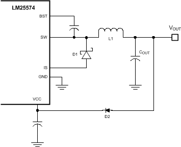
LM25574 20214118.gifFigure 18. VCC Bias from VOUT for 8V < VOUT < 14V
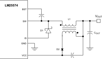
LM25574 20214119_nvs483.gifFigure 19. VCC Bias with Additional Winding on the Output Inductor