SNVS483H January 2007 – August 2017 LM25574
PRODUCTION DATA.
- 1 Features
- 2 Applications
- 3 Description
- 4 Revision History
- 5 Pin Configuration and Functions
- 6 Specifications
- 7 Detailed Description
- 8 Application and Implementation
- 9 Layout
- 10Device and Documentation Support
- 11Mechanical, Packaging, and Orderable Information
Package Options
Mechanical Data (Package|Pins)
- PW|16
Thermal pad, mechanical data (Package|Pins)
Orderable Information
8.1.12 R4, C5, C6
These components configure the error amplifier gain characteristics to accomplish a stable overall loop gain. One advantage of current mode control is the ability to close the loop with only two feedback components, R4 and C5. The overall loop gain is the product of the modulator gain and the error amplifier gain. The DC modulator gain of the LM25574 is as follows:
The dominant low frequency pole of the modulator is determined by the load resistance (RLOAD,) and output capacitance (COUT). The corner frequency of this pole is:
For RLOAD = 20Ω and COUT = 22µF then fp(MOD) = 362Hz
DC Gain(MOD) = 0.5 x 20 = 20dB
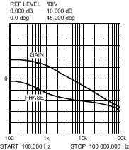
For the design example of Functional Block Diagram the following modulator gain vs. frequency characteristic was measured as shown in Figure 15.
 Figure 15. Gain and Phase of Modulator RLOAD = 20 Ohms and COUT = 22µF
Components R4 and C5 configure the error amplifier as a type II configuration which has a pole at DC and a zero at fZ = 1 / (2πR4C5). The error amplifier zero cancels the modulator pole leaving a single pole response at the crossover frequency of the loop gain. A single pole response at the crossover frequency yields a very stable loop with 90 degrees of phase margin.
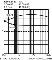
For the design example, a target loop bandwidth (crossover frequency) of 25kHz was selected. The compensation network zero (fZ) should be selected at least an order of magnitude less than the target crossover frequency. This constrains the product of R4 and C5 for a desired compensation network zero 1 / (2π R4 C5) to be less than 2 kHz. Increasing R4, while proportionally decreasing C5, increases the error amp gain. Conversely, decreasing R4 while proportionally increasing C5, decreases the error amp gain. For the design example C5 was selected for 0.022 µF and R4 was selected for 24.9 kΩ. These values configure the compensation network zero at 290 Hz. The error amp gain at frequencies greater than fZ is: R4 / R5, which is approximately 5 (14dB).
 Figure 16. Error Amplifier Gain and Phase
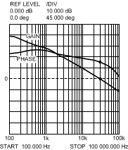
The overall loop can be predicted as the sum (in dB) of the modulator gain and the error amp gain.
 Figure 17. Overall Loop Gain and Phase
If a network analyzer is available, the modulator gain can be measured and the error amplifier gain can be configured for the desired loop transfer function. If a network analyzer is not available, the error amplifier compensation components can be designed with the guidelines given. Step load transient tests can be performed to verify acceptable performance. The step load goal is minimum overshoot with a damped response. C6 can be added to the compensation network to decrease noise susceptibility of the error amplifier. The value of C6 must be sufficiently small since the addition of this capacitor adds a pole in the error amplifier transfer function. This pole must be well beyond the loop crossover frequency. A good approximation of the location of the pole added by C6 is: fp2 = fz x C5 / C6.