SLVS569F January 2005 – August 2015 LM2575
PRODUCTION DATA.
- 1 Features
- 2 Applications
- 3 Description
- 4 Revision History
- 5 Pin Configuration and Functions
- 6 Specifications
- 7 Detailed Description
-
8 Application and Implementation
- 8.1 Application Information
- 8.2
Typical Application
- 8.2.1 Design Requirements
- 8.2.2
Detailed Design Procedure
- 8.2.2.1 Input Capacitor (CIN)
- 8.2.2.2 Output Capacitor (COUT)
- 8.2.2.3 Catch Diode
- 8.2.2.4 Inductor
- 8.2.2.5 Output Voltage Ripple and Transients
- 8.2.2.6 Feedback Connection
- 8.2.2.7 ON/OFF Input
- 8.2.2.8 Grounding
- 8.2.2.9 Reverse Current Considerations
- 8.2.2.10 Buck Regulator Design Procedure
- 8.2.2.11 Inductor Selection Guide
- 8.2.3 Application Curves
- 9 Power Supply Recommendations
- 10Layout
- 11Device and Documentation Support
- 12Mechanical, Packaging, and Orderable Information
Package Options
Refer to the PDF data sheet for device specific package drawings
Mechanical Data (Package|Pins)
- N|16
Thermal pad, mechanical data (Package|Pins)
Orderable Information
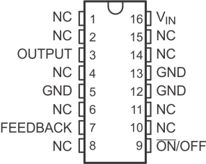
5 Pin Configuration and Functions

Pin Functions
| PIN | I/O | DESCRIPTION | |
|---|---|---|---|
| NAME | NO. | ||
| FEEDBACK | 7 | I | Output voltage sense |
| GND | 5 | — | Ground pins, all pins must be connect to ground. |
| 12 | |||
| 13 | |||
| ON/OFF | 9 | I | Active low enable |
| OUTPUT | 3 | O | Switch output |
| VIN | 16 | I | Input voltage supply pin |
| NC | 1 | — | Not connected internally, pins can be connected to circuit ground plane for improved thermal performance. |
| 2 | |||
| 4 | |||
| 6 | |||
| 8 | |||
| 10 | |||
| 11 | |||
| 14 | |||
| 15 | |||